2026-06-26 05:15:33
Hello you fine Internet folks,
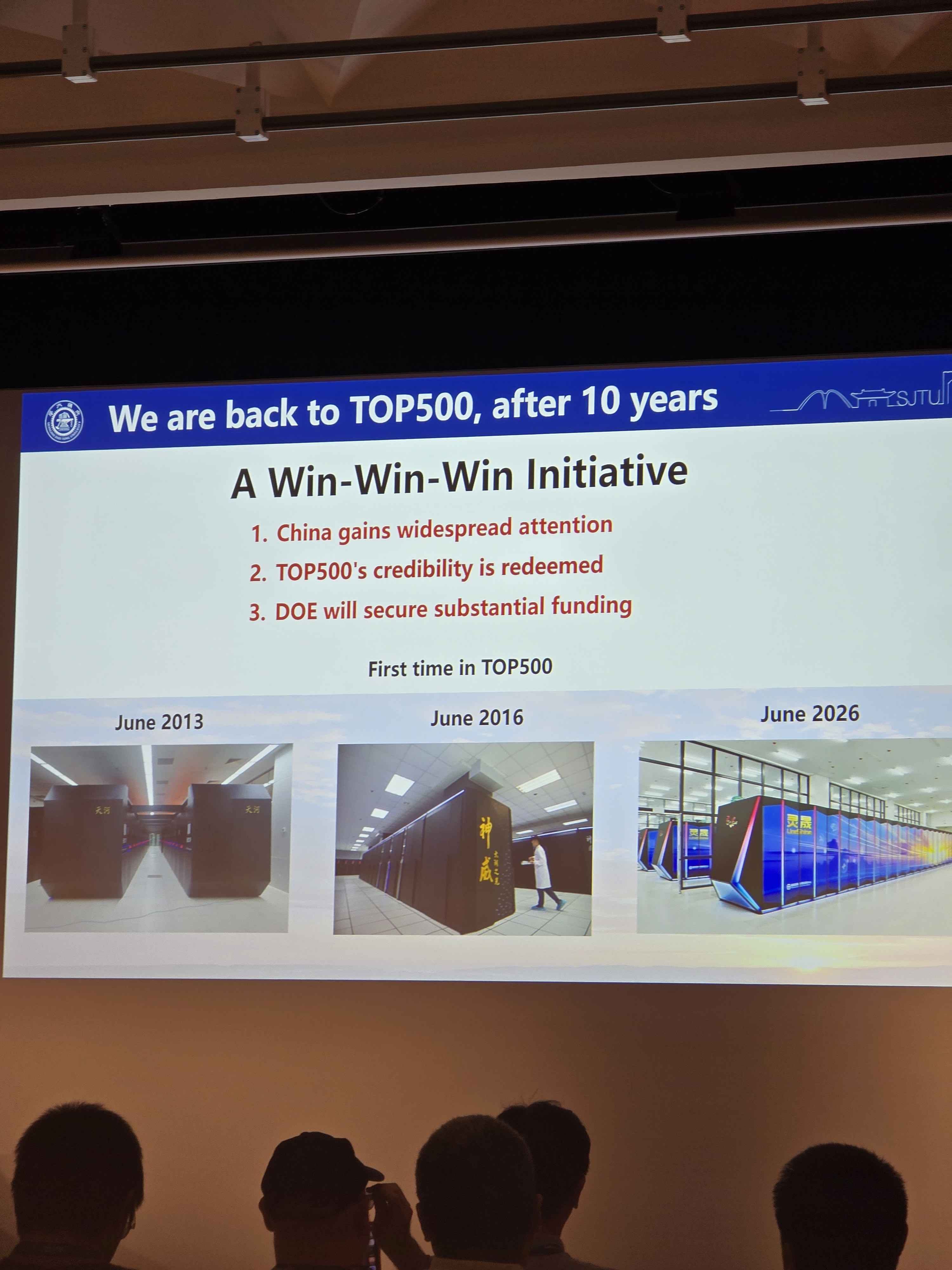
Here at ISC 2026 in Hamburg, Germany, we got the 67th TOP500 list where there was a surprise awaiting us. That surprise being a new Number 1 Supercomputer on the TOP500.
The new number one Supercomputer on the TOP500 list is the LineShine Supercomputer in Shenzhen, China. This is the first Chinese submission to the TOP500 in 9 years and they came in swinging with a massive CPU-only system.
Starting with the specifications of the CPU that powers the LineShine system, the LX2.
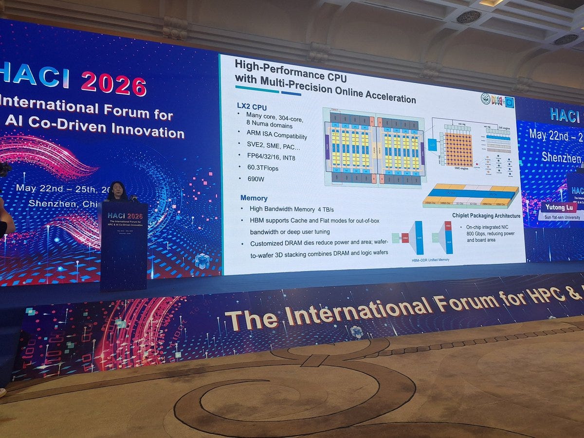
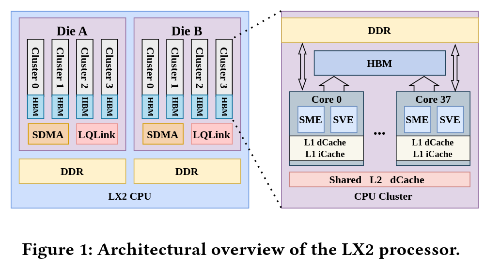
The LX2 is an Armv9-compliant CPU with support for SVE2 and SME. Each core has 32 KB of L1 instruction cache and 32 KB of L1 data cache. Physically, the chip is built from two compute dies, with each die containing four 40-core clusters. Two cores are disabled per cluster, leaving 38 active cores per cluster, or 152 active cores per die. Each cluster is backed by 28.5 MB of L2 cache, giving each die 114 MB of L2 and the full LX2 package 304 active cores with 228 MB of total L2 cache.
Those 304 cores run at 1.55 GHz and deliver a quoted 60.3 TFLOP/s of FP64 compute at 690 watts per LX2 CPU. The package also includes eight stacks of “high-bandwidth memory,” with 4 GB per stack for 32 GB of on-package high-bandwidth memory and 4 TB/s of bandwidth. However, this memory likely is not conventional HBM, despite being described in similar terms and could be an indigenous Chinese development. Because 32 GB is relatively small for a CPU of this scale, each LX2 is also backed by 256 GB of DDR5 memory that acts as a larger spillover tier.
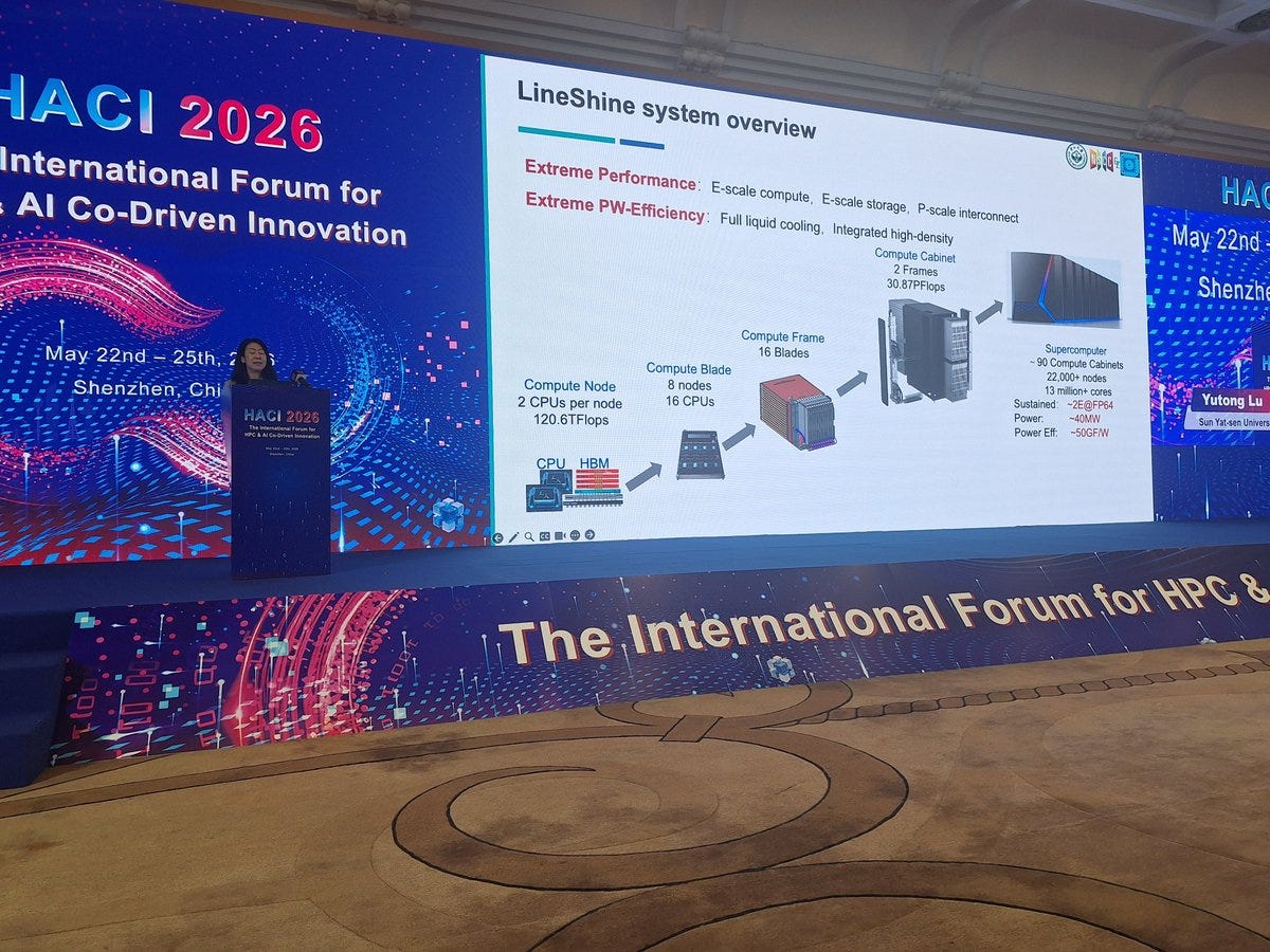
Transitioning from the CPU level to the node level, each node has two LX2 CPUs with 800 Gbps of networking for a total of 1.6Tbps of networking per node. 8 of these nodes are then combined into a compute blade, with 16 compute blades in a compute frame, and 2 frames per compute cabinet. In total the LineShine supercomputer has 90 compute cabinets which means that there are over 22,000 nodes and 13 million CPU cores in the full system.
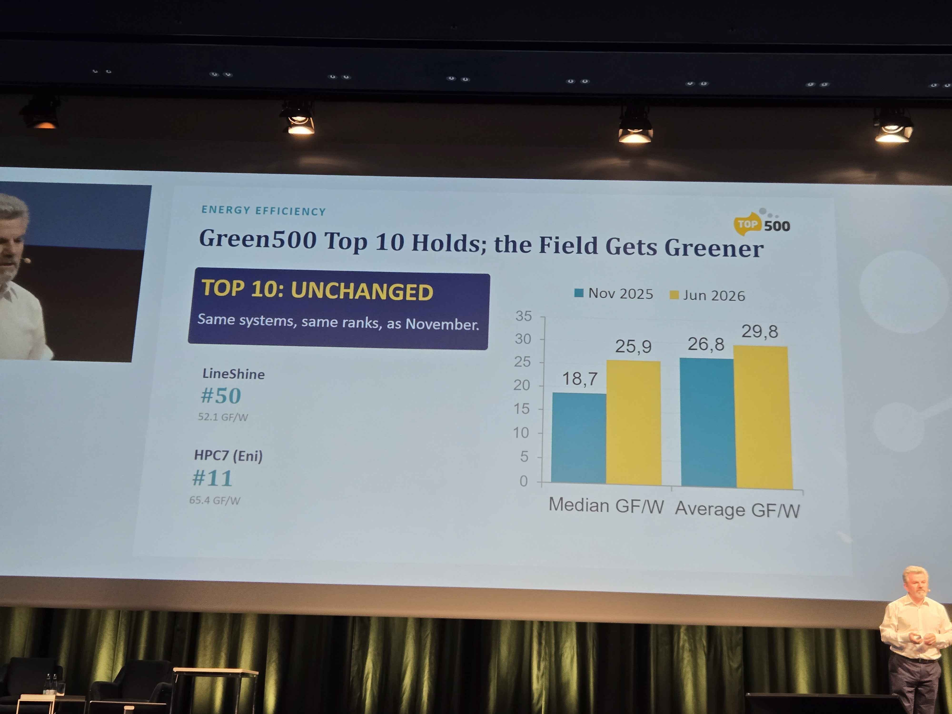
This puts the LineShine system at a total of 2.198 Exaflops of sustained FP64 (Rmax) out of an on-paper 2.735 Exaflops of FP64 (Rpeak). For this result, the LineShine system pulled 42.22 Megawatts of power for a FP64 efficiency of 52.07 Gigaflops per Watt, which, while it is well behind the leader of 73.282 FP64 Gigaflops per Watt, is very impressive for a CPU only system. And unlike prior Chinese Supercomputers, this system is not just a “LINPACK-special” but is also the number 1 in the HPCG benchmark with a result of 22.004 Petaflops per second beating out El Capitan’s 17.406 Petaflops per second result.
There is a new number 6 system on list, the HPC7 system from Eni in Italy. This is functionally El Capitan, just shrunk down to 30% the size. It is using the same HPE Cray EX4000 platform and AMD Instinct MI300A APUs, which is getting an Rmax of 571.5 Petaflops of FP64 performance out of an Rpeak of 861 Petaflops at 8.735 Megawatts of power consumed. With HPC7, Italy now has more compute listed on the TOP500 than any other country in Europe, despite Germany having Europe’s only Exascale system on the TOP500.
The former number 1 supercomputer, Fugaku, may have been pushed down to number 9 in the TOP500 ranking but it is still a lean, mean, science crunching machine. Despite being 6 years old, Fugaku is still number 3 on the HPCG list, which is a testament to the HPC focused design that Fugaku has, as it is still in the top 3 supercomputers as far as the HPCG list is concerned.
Moving to the Green500, there have been no changes to the Green500’s Top 10 list of most efficient supercomputers. This is the first time in the Green500’s history where there have been no changes to the Top 10 list. However that is not to say that HPC hasn’t gotten more efficient.
Due to retirements of older systems, the overall field of HPC has gotten more efficient in the past 6 months.
Personally, I wasn’t expecting to see a new number 1 on the TOP500, until either Discovery or Fukagu-Next was brought online. We have known that China has Exascale systems for a while now, but this is the first time that we have seen a China Exascale system on the TOP500.
This does beg the question of if China will also submit TOP500 results for their other exascale systems, Sunway Oceanlight and CNIS, or if they will keep those off of the TOP500 list.
I do wonder if this will cause the US Government to spend more money for large DOE systems and I am not the only one thinking that it could drive more money towards the DOE.
If the submission of LineShine ends up with the DOE getting more funding for more, and larger, supercomputers, then bully for us in the HPC community.
Something that is quite interesting is that Eni, an oil and gas company, has been submitting their systems to the TOP500 and they currently have 2 of the Top 10 systems on the TOP500. Which then begs the question, why aren’t the truly large AI systems, such as xAI’s Colossus 2 with over 550,000 Blackwell GPUs, on the TOP500? Why aren’t these AI companies submitting to the TOP500 to show off their computing prowess? To be honest, I don’t know why. A full HPL run on a supercomputer seems like a good way to stress all of the compute, memory, and networking of the system before declaring it to be operational.
There was one last key piece of news that came out of the TOP500 here at ISC 2026 and that is that the ISC Group will be handing over the TOP500 list to ACM SIGHPC moving forward. This functionally means that now all TOP500 lists will have dedicated DOI numbers which will make referencing specific TOP500 lists easier moving forward.
2026-06-12 13:13:37
Hello you fine Internet folks, today we have an interview with Kira Boyko, the Product Director of Intel Xeon 6+. Hope y’all enjoy!
Transcript below has been edited for conciseness:
George Cozma: Hello, you fine internet folks. We’re here at Computex 2026 at the Intel booth, or booth-room-floor area, whatever you want to...
Kira Boyko: Call it Intel space.
George Cozma: Yeah, well, whatever you want to call it. And I’m here with...
Kira Boyko: I’m Kira Boyko, and I am the product director for Intel Xeon 6+, which we have just launched at the event this week.
George Cozma: Now, starting off with a kind of simple question: what is a product director?
Kira Boyko: That is a good question. Actually, I get asked that somewhat frequently. A product director is someone who defines what the product is going to look like. So we look at the market requirements, what segments you want to target, how you want the product to perform, the different KPIs, and then you work all the way through to execution and delivery to make sure we are staying on track to our customers’ needs.
George Cozma: So are you actively saying, okay, this product needs to have at least X number of cores at X clock speed for X performance?
Kira Boyko: With X frequency, X application for this segment is going to need this KPI of performance. It needs to be able to support this and that, and this other part doesn’t matter. And then, working with our customers, of course, to answer those and understand their various applications, we build out models to ensure that we are supporting those appropriately.
George Cozma: Cool. And speaking of models, I assume you also are part of the SKU-ing, the people who decide what goes into, let’s say, the 6990...90+...E-Plus?...
Kira Boyko: 6990E+.
George Cozma: Okay, thank you.
Kira Boyko: Very confusing, yes.
George Cozma: And then, like, the SKUs down there, all the way down to the, I believe, the 6960E+.
Kira Boyko: Yes.
George Cozma: And so you determine what the gaps are and all that, or...?
Kira Boyko: Absolutely.
George Cozma: Okay. How are you doing all that? Are you just asking your customers what they want, or are you sort of just deciding through what can be cut down from different yields and whatnot?
Kira Boyko: It’s a combination of all the above. So it’s looking at all of our segments, understanding what those segments are going to need from an application perspective, and then determining how we best create SKUs to fit that. And then, of course, to your point, there is a lot of looking at the overall utilization to ensure that we are hitting our marks in terms of demand on a per-SKU basis.
But yeah, we try to keep it as simple as possible. Xeon 6+ has a simpler roadmap, which I’m particularly proud of, because Xeon honestly has a huge number. Yes. And we’re going to see a lot of crossover and application between some of our segments there, which is also going to help with the overall build and supply so that we have more material available for folks down the road to choose from.
George Cozma: Okay, excellent. And sort of, I guess, since you’re working with your customers, where in the design segment do you come in? Do you come in sort of as the product is being defined? So I guess before launch, how far back are you sort of involved?
Kira Boyko: Oh, years.
George Cozma: Okay, okay. So you’re sort of at the beginning.
Kira Boyko: Yes. Okay, yeah. The product manager actually starts out with the full product concept, or product kickoff, as well, right? So you start by saying, hey, this is what we need to deliver in this time frame. This is what we’re hearing from our customers. And then you start working with an architect and various other engineers to actually figure out how you’re going to build this and achieve it.
George Cozma: Okay. Now, sort of moving into Xeon 6+, the thing that really interested me the most was AET. Could you talk a little bit more about what that is, what the acronym is, and what that gives you over standard performance counters?
Kira Boyko: And we love a really good acronym. It is Intel Application Energy Telemetry, which you hopefully have, like, a sub-caption below this saying that, because...
George Cozma: I was like, when I first wrote it, I thought it was Advanced Energy Telemetry. I was like, wait...
Kira Boyko: I like that. I mean, sure, we can go with that too. I like that.
George Cozma: Should be XET. It didn’t just sort of fall into the everybody-has-an-X stuff.
Kira Boyko: That, and maybe a plus at the end, you know, just to make it super fun.
George Cozma: Or throw Ultra in the box as well.
Kira Boyko: Yeah, exactly. So it’s a new feature that we are introducing with 6+ that will be rolling out on all of our Xeons moving forward. So that’s important to know because, while 6+ is very focused on specific scalar workloads, we will have other CPUs, of course, that are focused on others, where this is going to be equally applicable. It is a feature that was highly requested by some of our customers.
So we developed that alongside feedback throughout the process. And it allows them to track, at a hardware core level, the actual energy usage of their workload as it’s moving from core to core. With that information, they can orchestrate differently so they’re using less energy. They can provide end-customer applications like visible chargeback to the actual energy utilized, or incentives with rebates to get them to utilize differently in order to reduce their energy consumption as well.
Previously, I believe there have been similar offerings that are on a software level, which adds additional tax and leaves space for misapplications, because it’s always different workloads that they’re tested on versus actually utilized by an end customer. So we’re really excited about this one. And it is available on all of our SKUs, which is great. And it works out of the box, so everyone can take advantage of it.
George Cozma: Cool. I assume it’s plumbed straight into perf?
Kira Boyko: Perf, from a metrics standpoint?
George Cozma: Yeah. Well, the performance counter suite, perf, in Linux.
Kira Boyko: Yes, yes, okay, yes. And it’s also compatible with all of our tools as well. Okay. So no additional work needed to be done to utilize that.
George Cozma: Are these hardware-level sensors, or is this like software modeling? So I know, for example, on laptops, instead of sometimes what you do is you actually just sort of model what the power should be instead of having an actual counter. Is this like hardware sensors embedded into the Xeon processor for this?
Kira Boyko: It is. It is a hardware-level hook into the core that allows tracking.
George Cozma: Okay. And then how, I guess, so Xeon 6 is you have effectively 72 clusters of four cores. How is it at the core level, or is it at the cluster level? Okay. Can you also get cluster-level monitoring as well?
Kira Boyko: I would have to check. I imagine that can certainly be viewed through it, but we’ll check and we’ll get back to you, okay.
George Cozma: Because, I’m sorry, zooming out from there, it’s not only do you have that cluster, you then have the whole SoC, you have the uncore and stuff. So I was asking if you could monitor the power of the entire system, sort of.
Kira Boyko: Oh, yes.
George Cozma: Okay. So all the way from the package level straight down into the single-core level. Okay, cool. It’s always great. You get more data points.
Kira Boyko: Yeah, yeah.
George Cozma: And more hardware sensors as well, also really fun to measure. What power differences can you get from an integer workload versus an FP workload and all that fun stuff? And you said moving forward, next-generation Xeons and continuing on will have this, are you thinking about potentially, I know this may not be your area, bringing that down into the consumer realm and sort of plumbing that into consumer devices as well?
Kira Boyko: Yeah, not my realm on the consumer side. But we do usually share information about our features that we’re building on the datacenter side to see if there’s application and use for clients.
George Cozma: Okay, awesome. Because I guess another question is, sort of continuing on that, how much do server and client talk to each other in terms of not just technology, but the sharing of different written knowledge?
Kira Boyko: Oh, quite a bit. Yeah, we’re very transparent. If they’re doing something super cool over there, we want to know if it can be applied to our space, and vice versa. We also have a lot of open dialogue around new features that we have coming out to support specific cores that are going to cross over. For example, 6+ is the first 18A Xeon. There’s also an 18A client that already launched.
George Cozma: Which just so happens to be in my bag.
Kira Boyko: Awesome. So we do a lot of cross-pollination to see where we can best leverage our resources and make sure that we are supporting the feature sets that are right for both of our audiences, as well as separately too.
George Cozma: Okay. I guess that leaves me with one final question, the most important question of this interview: what’s your favorite type of cheese?
Kira Boyko: I love blue cheese, specifically because I am a blue-cheese-stuffed-olive-in-a-martini person, so I’ll say that.
George Cozma: Blue cheese is not my personal favorite, but I have to respect people who enjoy it.
Kira Boyko: Are you going to share your [favorite cheese]?
George Cozma: It’s cheddar and my favorite as of late has been, because I just got it, somebody from Oregon just sent it to me, Tillamook 12-year cheddar. Oh, so good. But I have been getting into Manchego, so sheep’s cheese, so sheep’s milk cheese, which is a lot more sort of fatty, and...
Kira Boyko: Have you tried goat milk cheddar?
George Cozma: Cheddar? Yes, I have. Goat milk cheese, for me, is a bit hit or miss. It depends on how it’s been done. But I really like Humboldt Fog from Cypress Grove.
Kira Boyko: I know that one. Yep, delicious.
George Cozma: Yep, yep, I’m with you. Well, thank you so much for sitting down to interview sort of last minute. But thank you so much for watching. If you like interviews like this, hit like, hit subscribe. It does help, as much as it pains me to say it, to show the like and subscribe buttons. But if you would like a transcript of this, that will be on the Chips and Cheese Substack, along with links to our Patreon and PayPal. Thank you so much, folks. Have a good one.
2026-05-23 16:40:38
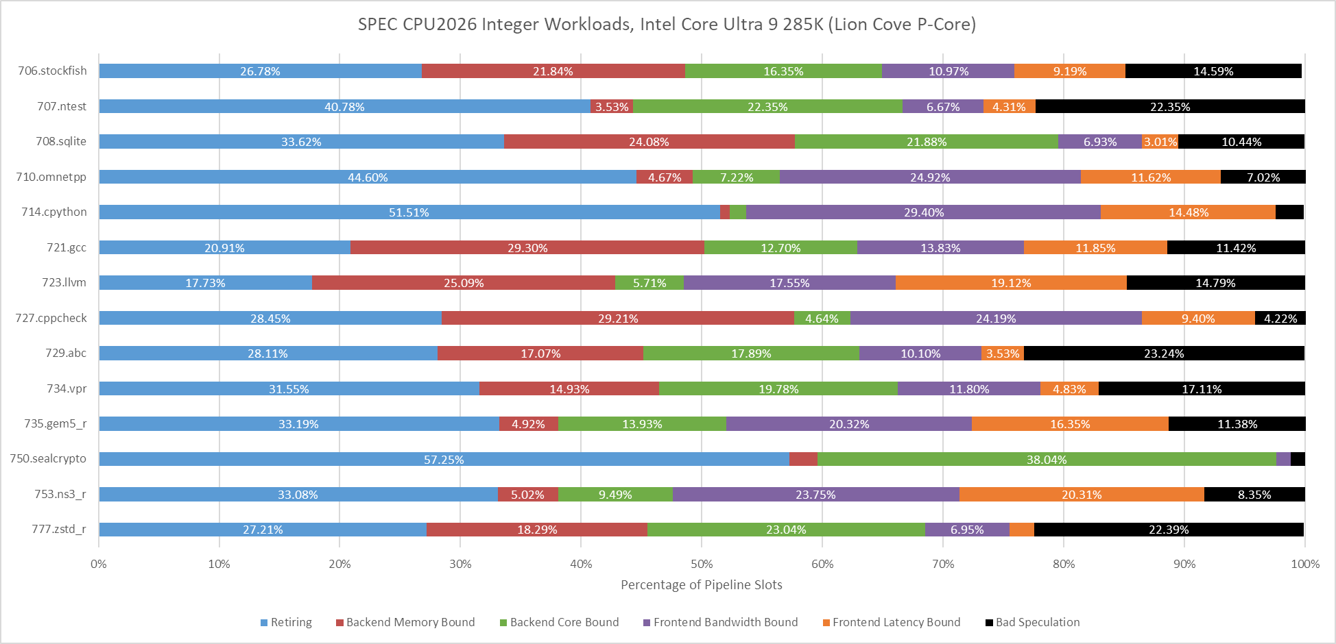
SPEC’s CPU benchmark suite has been a long established industry standard, and is almost impossible to miss when reading through various publications. Intel used SPEC CPU2000 to showcase Pentium 4’s improvements over Pentium III. Samsung used SPEC CPU2000 and SPEC CPU2006 traces to tune their Mongoose cores. SPEC CPU2017 formed part of Intel’s performance projections for Lion Cove. Now, SPEC has updated their CPU benchmark suite with SPEC CPU2026. The new suite consists of 52 workloads, up from 43 in SPEC CPU2017. Individual workloads consist of more source code lines, measured in KLOC (thousands of lines of code). SPEC’s goal is to modernize their CPU benchmark suite, while retaining the portability goals that characterized SPEC.
Because of SPEC’s importance in the CPU performance world, I’ll be looking over the new suite’s workloads to examine the challenges that they serve up to CPUs. I’m interested in hardware rather than compiler comparisons, so I’ll be using GCC 14.2.0 with -O3 and native architecture/optimization targets. I did try GCC 15.2.0, but ran into various issues and decided to stick with GCC 14.2.0 to conserve time. I’m testing all of the systems below using Linux.
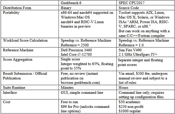
SPEC CPU scores represent speedup ratios relative to a reference system. Each SPEC CPU update tends to update the reference system, though not always to one that’s a relevant comparison for recent hardware.
An Ampere eMAG 8180 system provides the reference score of 1.0 for SPEC CPU2026. Ampere’s eMAG is faster than the Sun Fire V490 used for SPEC CPU2017, in much the same way that a Cessna 172 might be faster than a Sopwith Camel. Neither is a good comparison against modern airliners. Similarly, Ampere eMAG was not a widely deployed platform, and even systems that pre-date it by many years outperform it by a large margin. I’ve heard part of the motivation behind using a slower system was to let most systems achieve high scores, but that could have been accomplished by making the reference score a higher number, like 1000, instead of 1.0. Geekbench 6 takes a more reasonable approach, with a Core i7-12700 calibrated to a reference score of 2500. Unlike Ampere’s eMAG, Intel’s Core i7-12700 and similar CPUs were widely deployed across consumer systems, and Intel today uses a similar core architecture in Xeon 6.
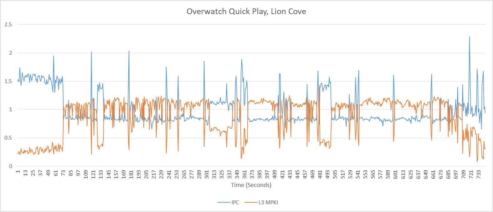
Examples of Intel and AMD’s latest desktop CPUs show similar performance in SPEC CPU2026’s integer suite, while Zen 5 tends to pull ahead in floating point tests. I had to run SPEC CPU2026 on a Lion Cove core that only reached 5.5 GHz, because the two 5.7 GHz capable cores had trouble completing the test suite without crashes. There seems to be something wrong with my sample, but I suspect a Lion Cove core that does complete the tests at 5.7 GHz would narrow the gap.
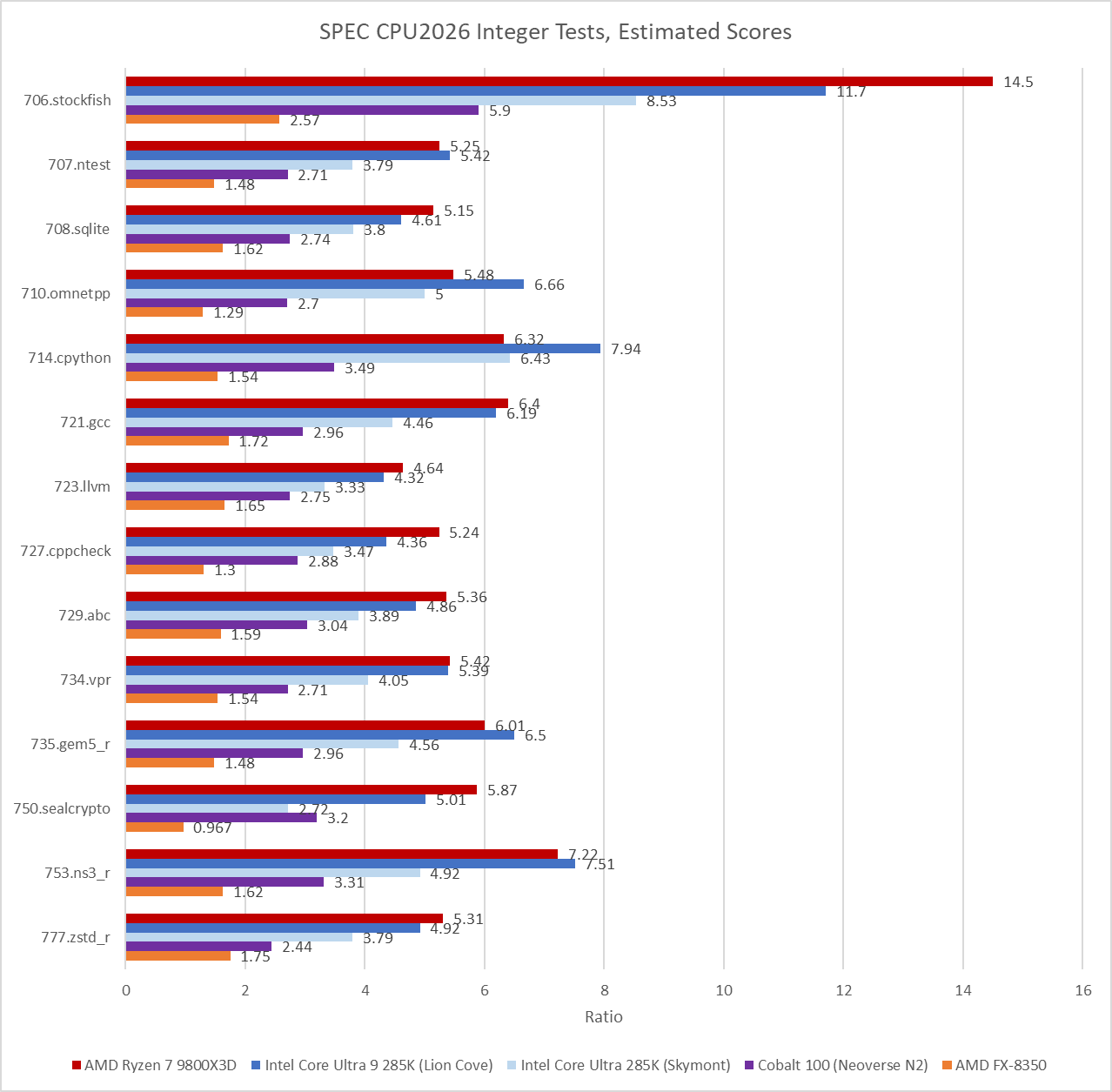
Individual scores in the integer suite show Zen 5 and Lion Cove closely matched, as the aggregate scores would suggest. Absolute scores show just how far outmatched the Ampere eMAG system is. Current desktop cores obliterate ones in the Ampere eMAG, especially in 706.stockfish. Even the FX-8350, which is over a decade old, might be a better reference point. It also sails way past the eMAG system in nearly every test.
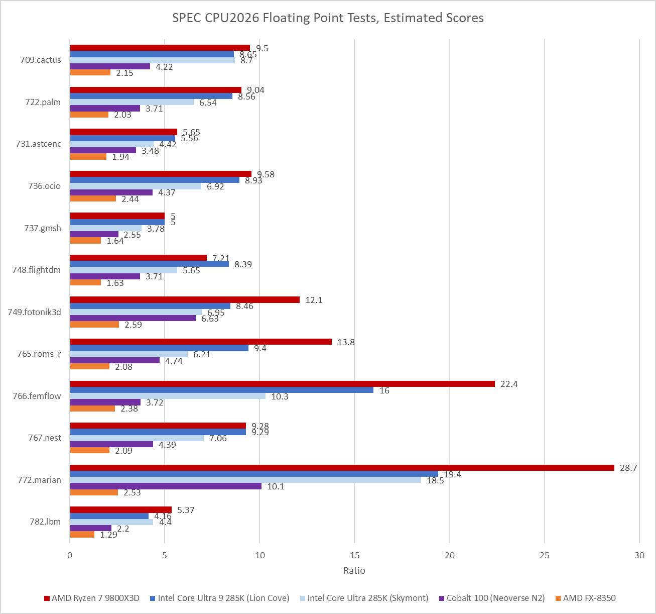
Floating point workloads are even worse for the old eMAG system. Zen 5 has a field day in several of the floating point workloads. Some of that is because GCC was able to generate AVX-512 instructions. I used Intel’s Software Development Emulator to get instruction counts for the last invocation of each workload, to give an idea of what instruction types are in use. Some SPEC CPU2026 tests run multiple commands to test the same binary against different input data, but I only profiled the last invocation to save time.
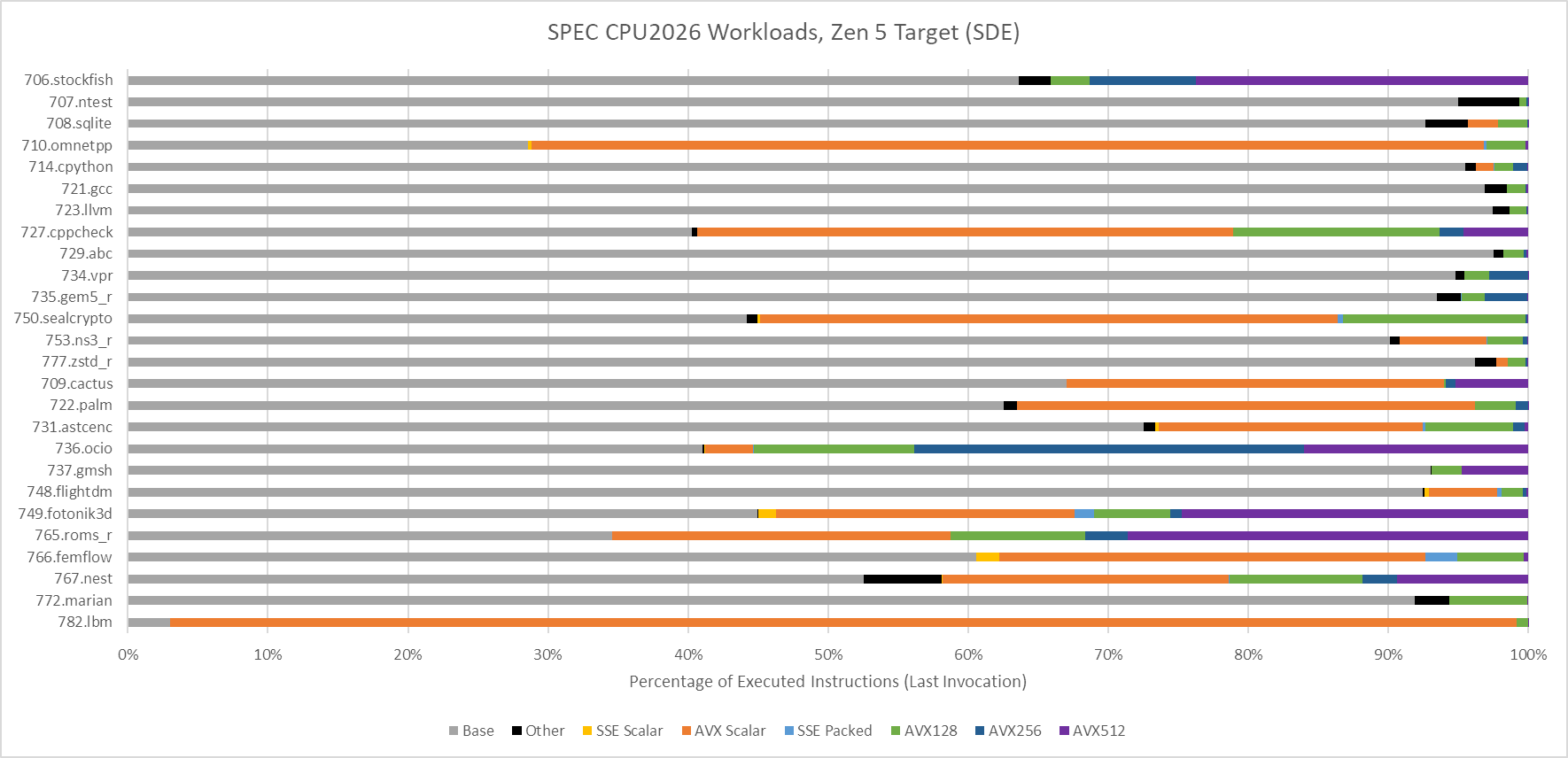
706.stockfish, 749.fotonik3d, and 765.roms all include AVX-512 code when compiled with GCC 14.2.0. Several other tests take advantage of 128-bit or 256-bit vectors too.
Average IPC, or instructions per cycle, gives a rough idea of how well CPU cores can bring their execution resources to bear. Low IPC often indicates cache misses, branch mispredicts, or less commonly, specific performance hazards in a core’s architecture. High IPC suggests performance is limited more by execution latency, execution resources, or core width. IPC of course shouldn’t be confused with actual performance, which depends on clock speed as well as work done per instruction.
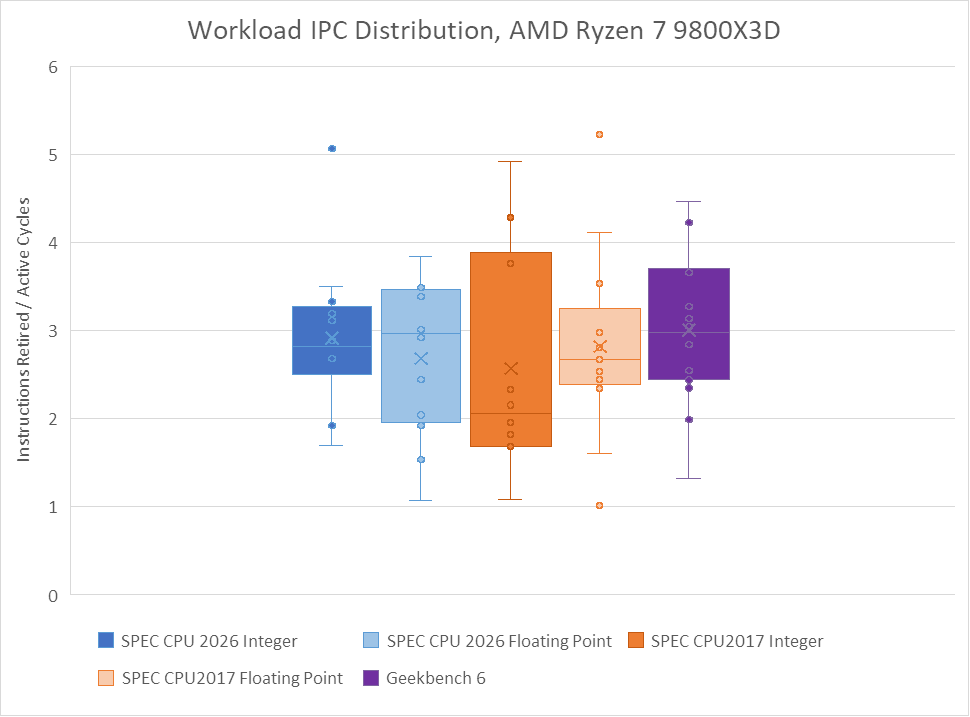
SPEC CPU2026’s integer suite displays a higher and tighter IPC distribution than SPEC CPU2017’s integer suite on both AMD’s Zen 5 and Intel’s Lion Cove. The IPC spread feels close to that of Geekbench 6, which tends to emphasize core throughput with few branch mispredicts or last level cache misses.
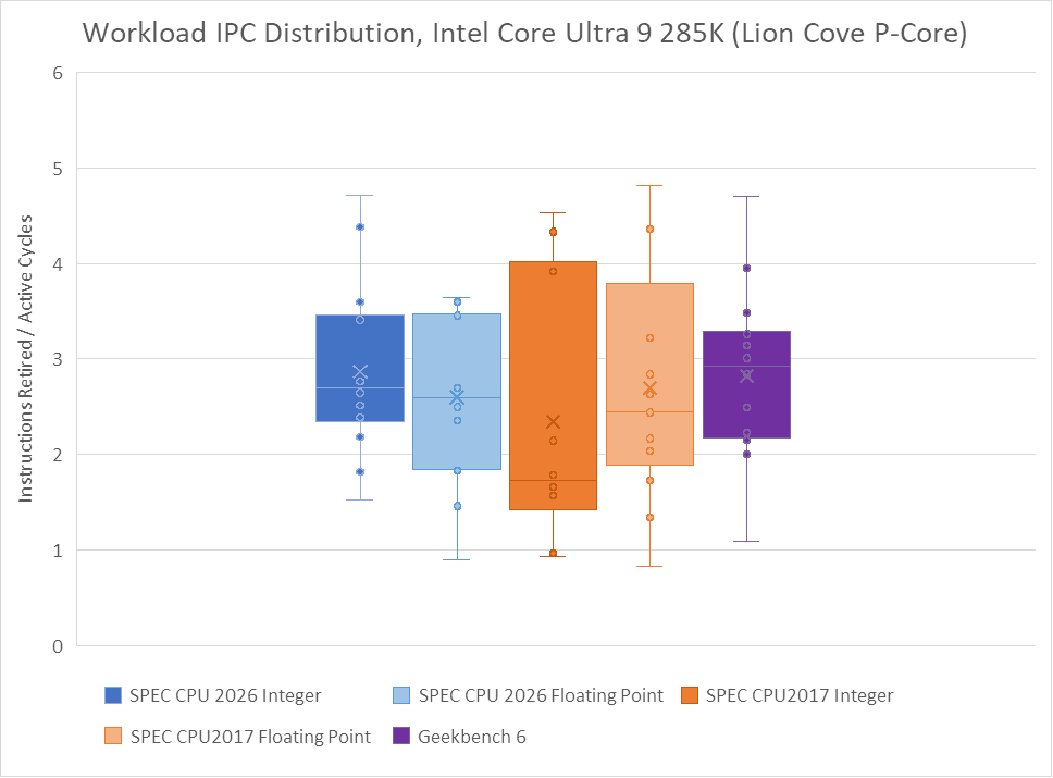
Floating point workloads get a wider spread on Zen 5 with the updated suite, while SPEC CPU2017’s floating point tests tended to bunch up around 2-3 IPC. Lion Cove had a wider IPC spread with the older floating point suite, and continues to see a wide spread in the new one.
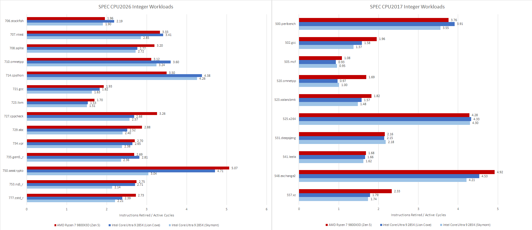
505.mcf and 520.omnetpp were low IPC workloads in SPEC CPU2017. Both suffered plenty of cache misses, and 505.mcf suffered a lot of branch mispredicts too. Neither test has an equivalent in SPEC CPU2026’s integer suite. MCF is gone, and 710.omnetpp is a completely different animal despite sharing the same name as the old test. Two code compilation tests, 721.gcc and 725.llvm, take over as the lowest IPC integer tests. They still average above 1.5 IPC though, which isn’t too low. For perspective, most PC games average around 1 IPC.
On the other hand, SPEC CPU2026’s integer suite includes plenty of high IPC workloads. More than half average close to 3 IPC if not beyond. 750.sealcrypto reaches the highest IPC across all integer workloads on both Zen 5 and Lion Cove. It’s also a high IPC workload on the Skymont E-Core, if just a little less so.
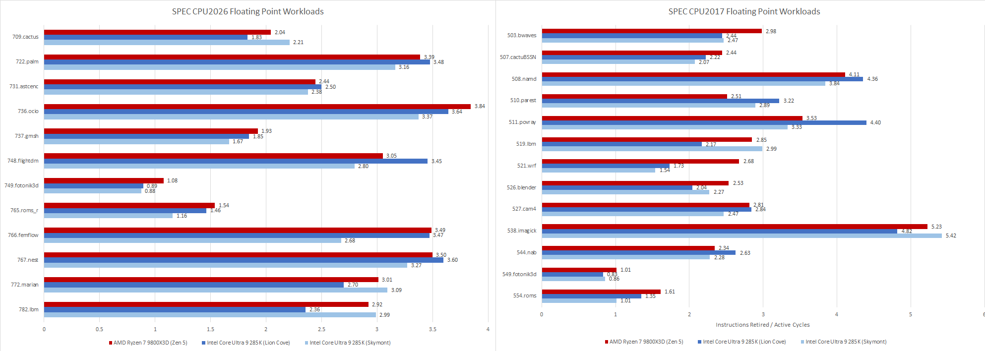
SPEC’s floating point workloads tend to focus on core throughput, and that remains the case with SPEC CPU2026. Many workloads sit above 2 IPC, which I consider a medium to medium-high IPC range. 749.fotonik3d and 765.roms fill the same role as their SPEC CPU2017 counterparts, and continue to stress DRAM performance by often missing in the last level cache. At the high IPC end, 538.imagick is gone with no direct replacement. Several SPEC CPU2026 floating point workloads do average well above 3 IPC, but none go as astronomically high as 538.imagick did.
Top-down analysis attributes under-utilized core width to various reasons, and provides a high level overview of where potential core throughput is being lost. It works at the rename/allocate stage, which is typically the narrowest part of a CPU’s pipeline that all instructions must pass through. Each pipeline slot at that stage is classified as follows:
Retiring: Slot was used by a micro-op that ultimately retired, meaning its results were made architecturally visible after passing all checks. Retired micro-ops represent useful work.
Backend Bound: A micro-op was available from the frontend, but couldn’t be sent to the backend because a required out-of-order tracking resource wasn’t available. That could mean the reorder buffer, register files, or memory ordering queues didn’t have a free entry when one was needed.
Frontend Bound: The frontend didn’t supply enough micro-ops to feed all renamer slots
Bad Speculation: A micro-op went through the slot, but wasn’t retired. This represents wasted work, for example from branch mispredicts
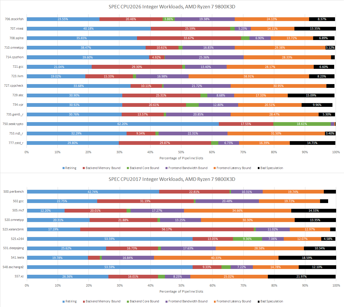
Retiring slots are up across the board compared to SPEC CPU2017’s integer suite, which is expected given the higher IPC figures seen above. 723.llvm and 721.gcc are mostly held back by frontend latency, which is classified as cycles where the frontend didn’t supply any micro-ops to the renamer. Both 723.llvm and 721.gcc are branchy workloads and occasionally suffer mispredicts, which interrupts the frontend’s ability to follow the instruction stream and smoothly deliver micro-ops. At the other end, 750.sealcrypto barely has any branches. Both Lion Cove and Zen 5 blast through it unimpeded, since there’s not much slowing their backends either.
SPEC CPU2017’s floating point workloads tend to focus more on core throughput, and that continues to be the case in SPEC CPU2026. Branches tend to be rare and predictable, letting the frontend on Lion Cove and Zen 5 operate with high efficiency.
Fotonik3d and roms are heavily backend memory bound on both Lion Cove and Zen 5. Most other tests are core-bound, though there are exceptions. Both Lion Cove and Zen 5 are challenged in similar ways, except for 709.cactus. In that test, Zen 5 is bound by frontend bandwidth, meaning the frontend delivered some micro-ops but not enough to fill all eight renamer slots.
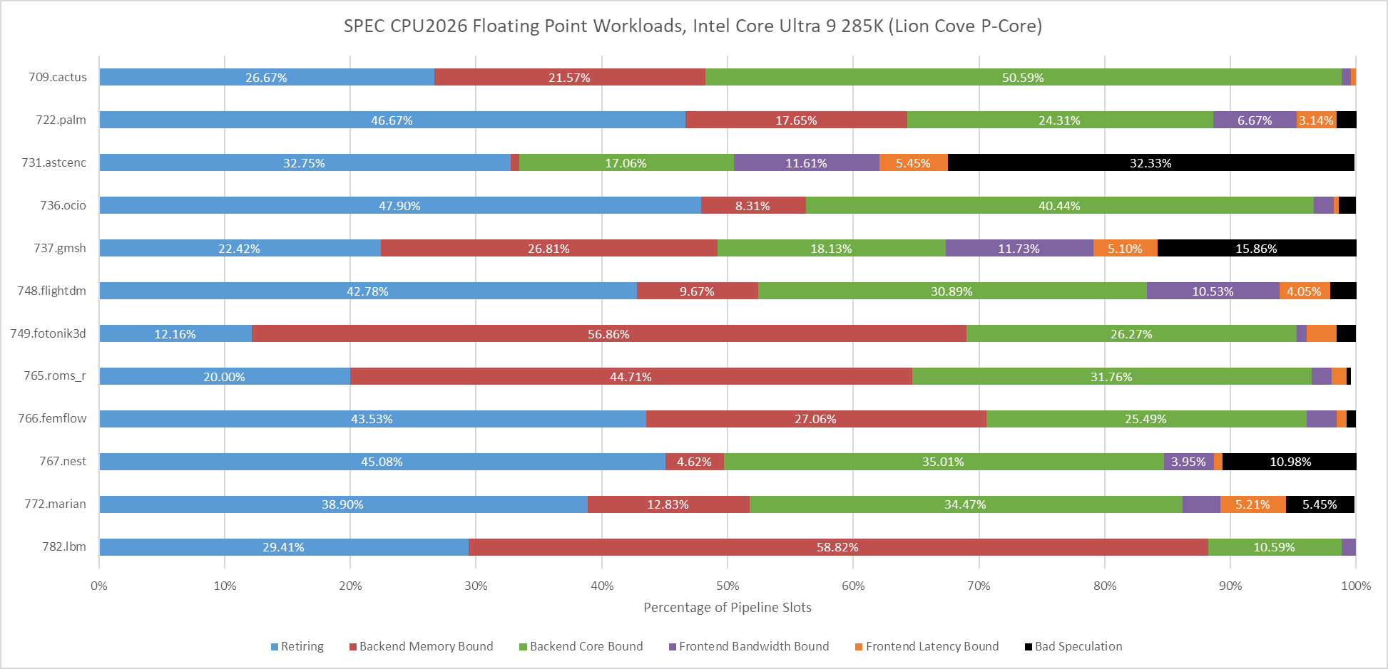
Lion Cove’s frontend has a field day in 709.cactus, but the core runs into backend limitations and overall Intel isn’t able to pull ahead of AMD.
Branch prediction has been a key challenge in designing high performance CPUs for decades. SPEC CPU2017’s integer tests were often challenging from a branch prediction perspective, even for modern cores with sophisticated branch predictors. 505.mcf, 541.leela, and 557.xz all suffer plenty of mispredicts on AMD’s Zen 5. Those tests would reward CPUs with better branch prediction, faster branch resolution, and the ability to hide mispredict penalties behind other work.
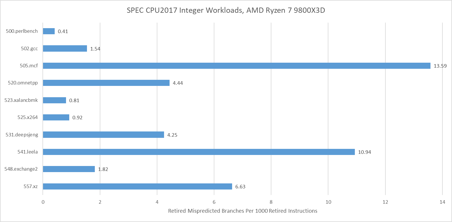
SPEC CPU2026’s integer suite places less emphasis on branch prediction. 721.llvm remains a moderate challenge, but suffers fewer mispredicts per instruction than 557.xz, to say nothing of 505.mcf and 541.leela. Lower difficulty on the branch prediction side contributes to higher IPC averages.
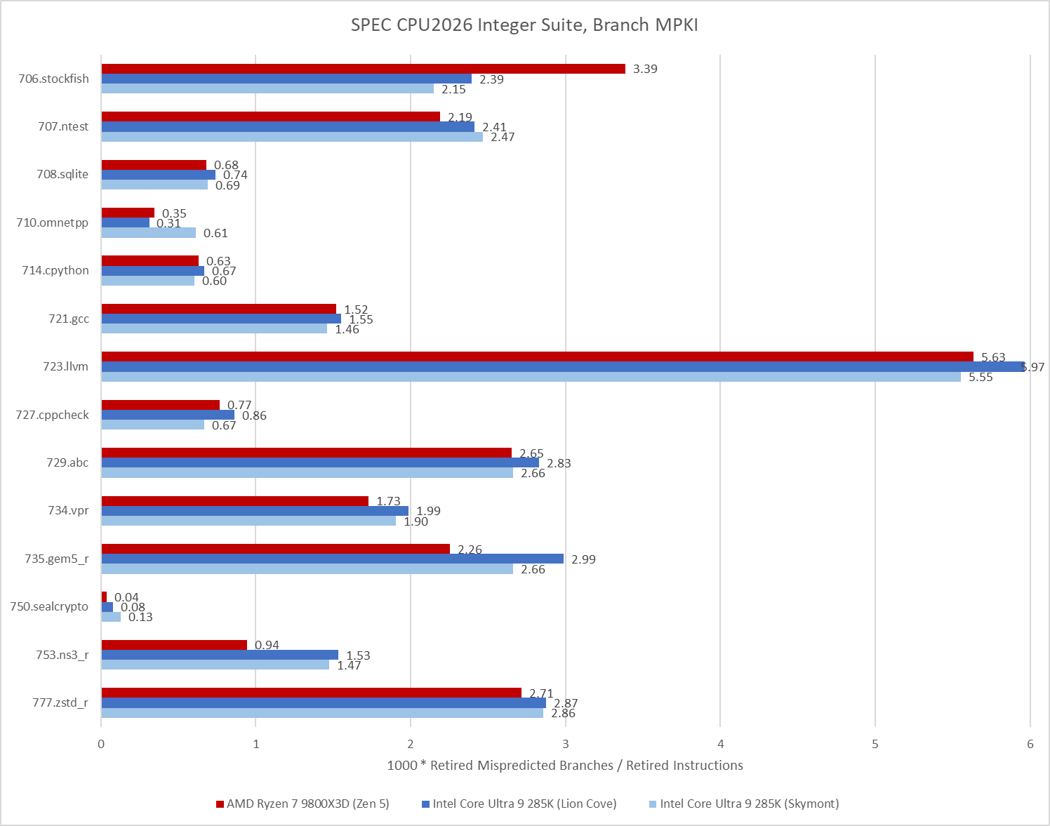
Floating point workloads in SPEC CPU2017 tend to be less challenging for branch predictors, though not always. 526.blender did lose throughput to bad speculation, but SPEC CPU2017’s floating point tests didn’t get close to 557.xz, 505.mcf, or 541.leela in terms of branch prediction difficulty.
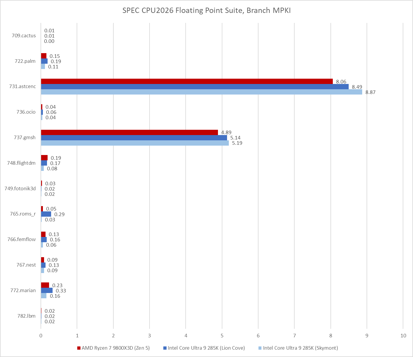
SPEC CPU2026 moves the needle on that, with 731.astcenc stepping up as the single biggest branch prediction challenge across both the integer and floating point suites. It’s still not as big of a challenge as 505.mcf from SPEC CPU2017’s integer suite, but it should still suffice to represent a workload with unpredictable control flow.
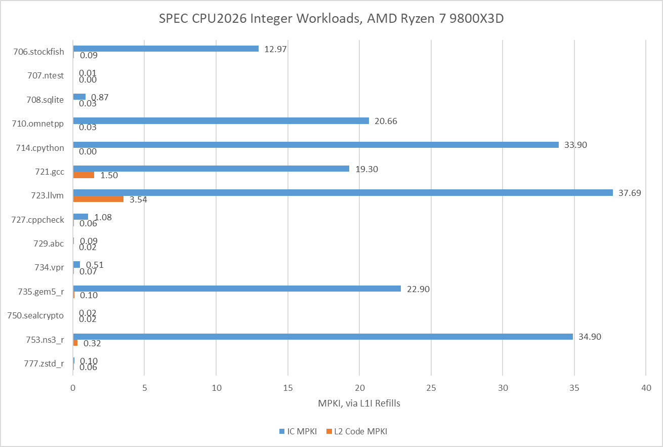
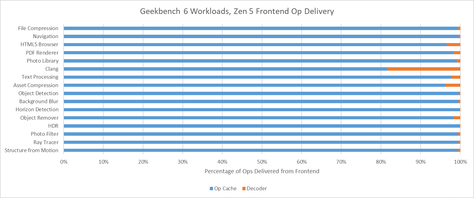
Good caching is important for instructions as well as data. AMD’s recent cores lean towards optimizing for small instruction footprints, and seek to capture much of the instruction stream in a highly optimized micro-op cache. SPEC CPU2026’s integer suite challenges that approach more than SPEC CPU2017’s did. Several workloads have less than 80% op cache coverage, so it appears that SPEC’s move to workloads with more source code lines sometimes correlates with worse code locality. Still, Zen 5 is able to mostly run code out of its op cache, and the decoders don’t see much use.
Further down the cache hierarchy, many of the tests with less than 90% op cache coverage see significant L1 instruction cache misses too. AMD has stuck with a 32 KB L1 instruction cache ever since Zen 2 which doesn’t offer too much extra coverage over the op cache. In nearly all tests, the 1 MB L2 cache is enough to capture the vast majority of L1 instruction cache misses. Only the two code compilation workloads see a noticeable degree of code fetches that miss L2, which could contribute to their lower IPC.
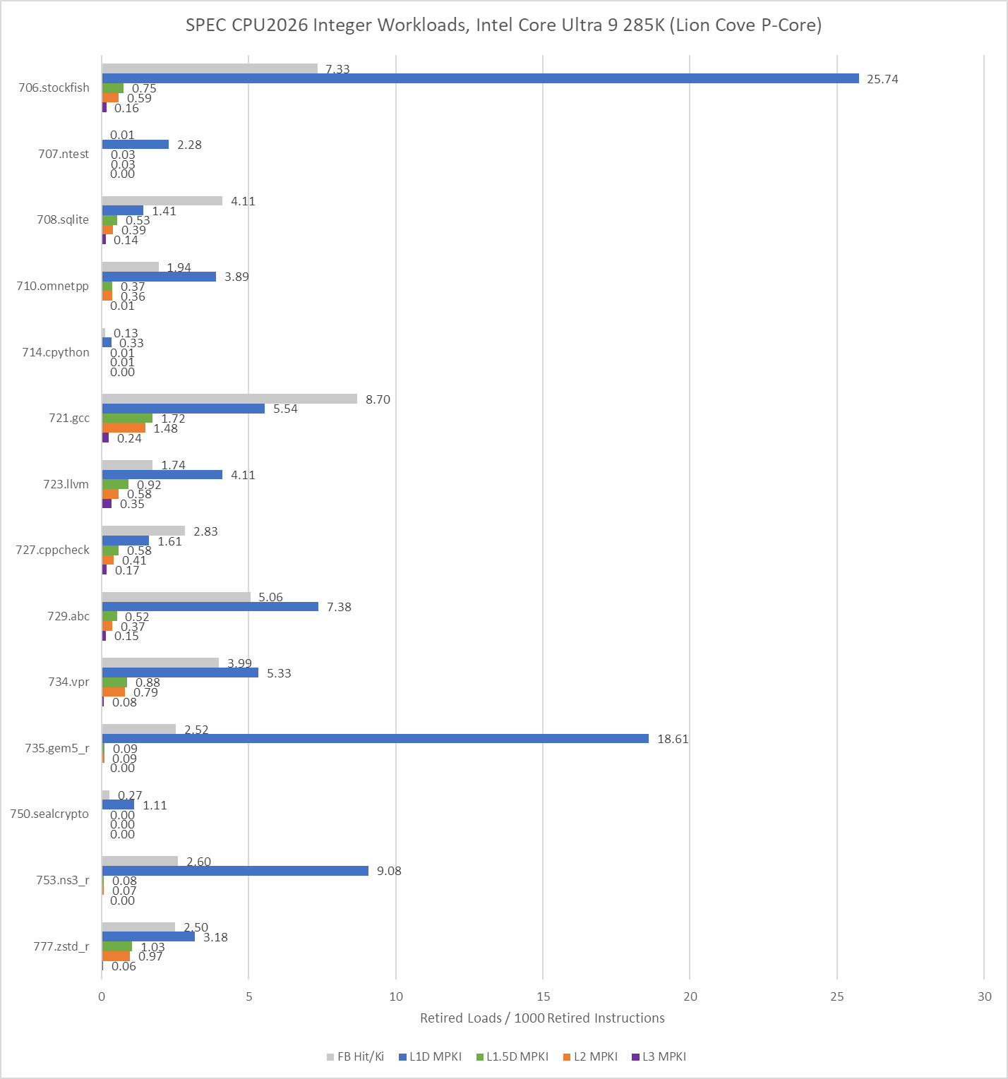
Intel takes a different frontend approach, with a smaller 5.2K entry op cache backed by a larger 64 KB instruction cache. Intel also uses a 8-wide decoder, which can provide higher instruction bandwidth to a single thread for large code footprints than AMD’s 4-wide, per-thread decoders. Lion Cove’s larger instruction cache suffers fewer misses across the board, and nearly eliminates code fetches from L2 in 714.cpython and 706.stockfish. Where the L1 instruction cache does see a significant number of misses, Lion Cove’s huge 3 MB L2 is able to step in and largely prevents code fetches from going through to L3.
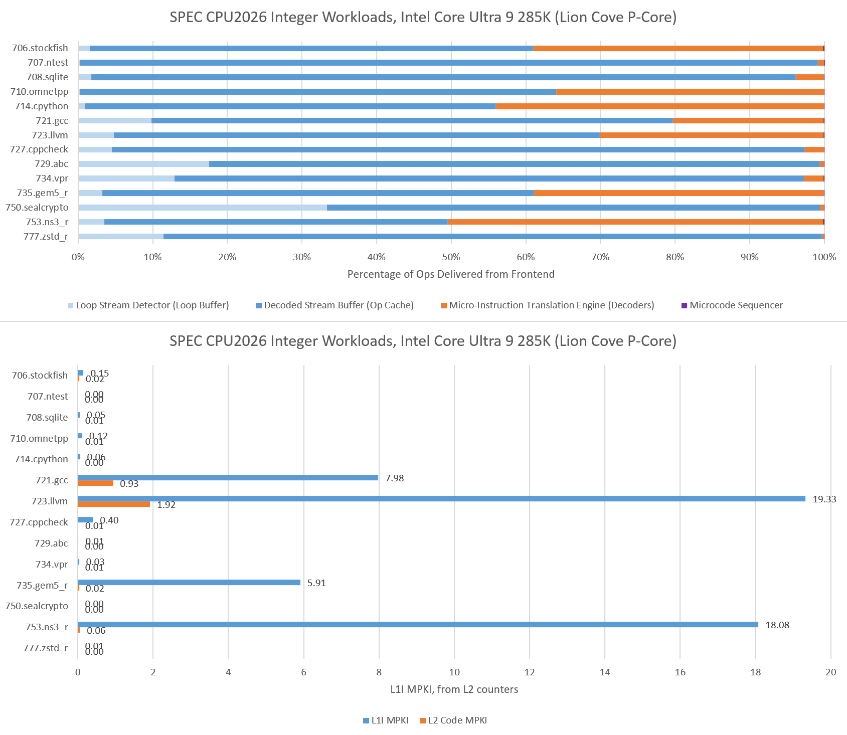
For very small code footprints, Intel has a Loop Stream Detector that locks down the micro-op queue and uses it as a loop buffer. The LSD plays a minor role in most integer tests, except for 750.sealcrypto.
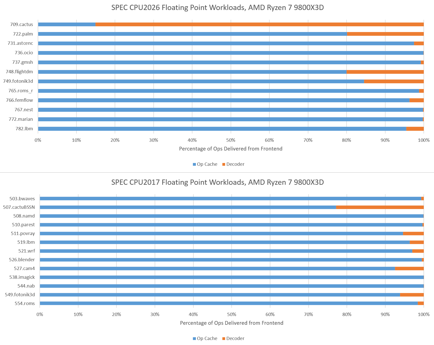
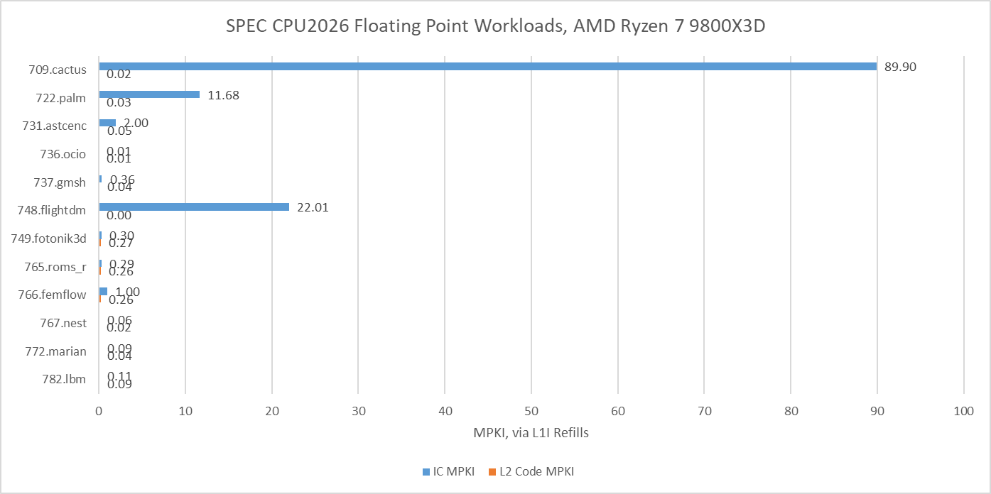
SPEC CPU2017’s floating point suite tended to be core throughput focused, with smaller instruction footprints than their integer counterparts, with exceptions of course. SPEC CPU2026’s updated floating point suite has more of those exceptions, and tougher ones too. 709.cactus has Zen 5 mostly feeding itself from its decoders, which explains why top-down metrics showed it as being frontend bandwidth bound. As with the integer suite, tests with lower op cache coverage tend to also miss in L1i. 749.fotonik3d doesn’t though. It spills out of the op cache more than its identically named predecessor in SPEC CPU2017, but all of that is caught by Zen 5’s L1 instruction cache.
LSD data from Lion Cove shows that many floating point tests spend a lot of runtime in tiny loops. 722.palm is a funny case, with Lion Cove’s 192 entry micro-op queue achieving over 40% coverage. Then once it gets out of that loop, it has a good chance of missing the op cache and the 64 KB L1 instruction cache.
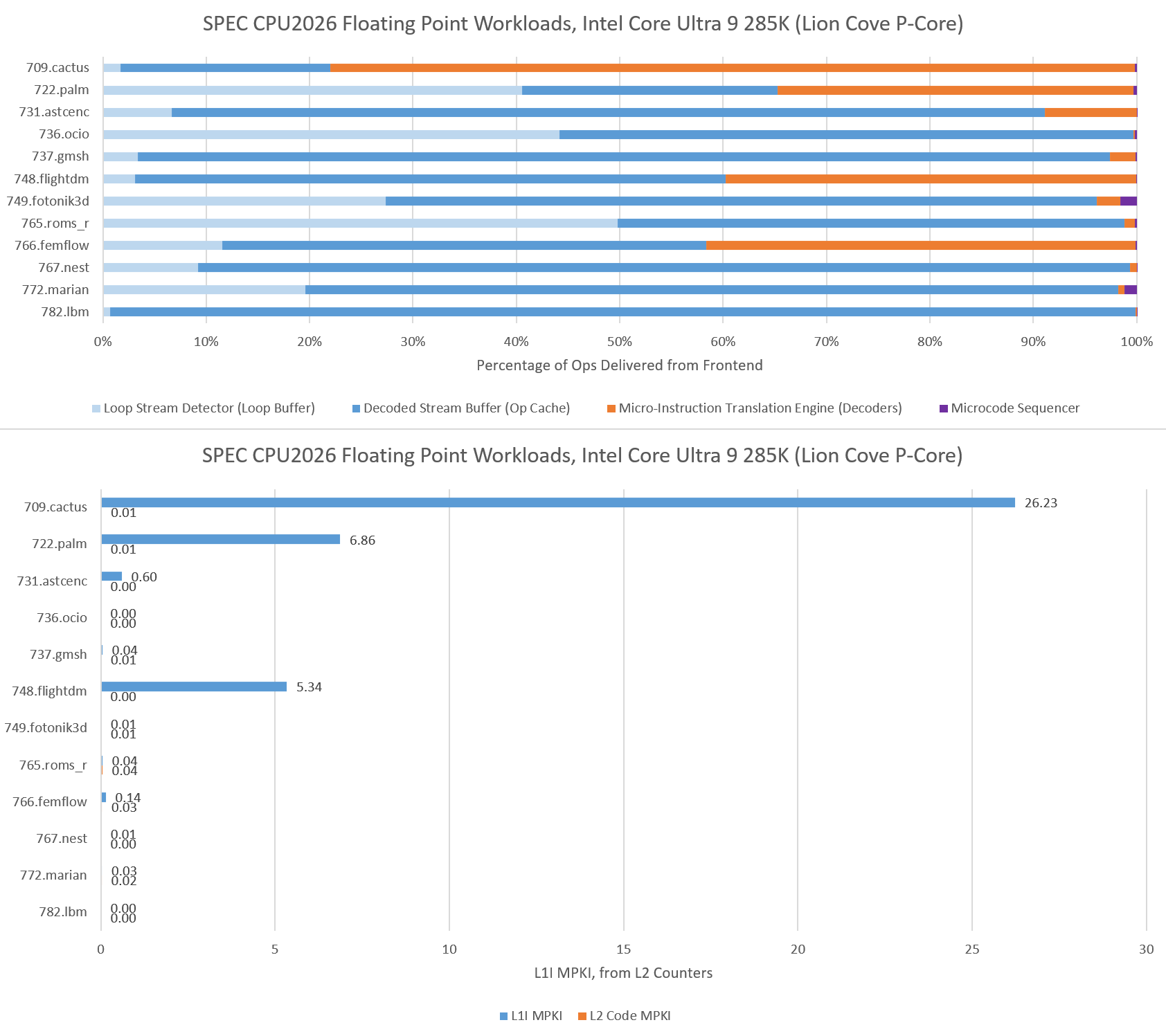
None of the floating point workloads presents enough of a challenge on the code footprint side to spill out of L2.
Data accesses that miss cache present another performance limiter for modern CPUs, especially for PC games. SPEC CPU2026’s integer suite has plenty of workloads that often miss in a 48 KB first level cache, and many that challenge a 1 MB L2 as well. However, the integer suite is light on workloads that encounter last level cache demand misses.
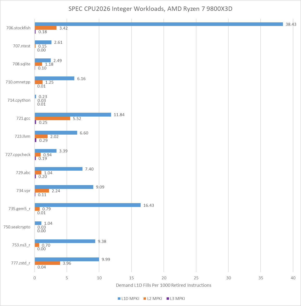
714.cpython and 750.sealcrypto rarely miss even in Zen 5’s L1D cache, which explains their high IPC alongside other factors.
Lion Cove performance counter data does a good job of justifying its 192 KB L1.5 data cache. As it turns out, quite a few workloads with significant L1D misses have nearly all of those misses contained within 192 KB. Last level cache misses are rare, suggesting a 36 MB cache is sufficient for many of SPEC CPU2026’s integer workloads.
On the floating point side, 709.cactus is prickly for a 48 KB L1 data cache, but Zen 5’s larger caches do a good job of cleaning up the misses. AMD’s L2 and L3 caches do well in general across the floating point suite. Only 765.roms and 759.fotonik3d have significant last level cache miss activity.
L3 MPKI figures are lower on Intel, but those don’t tell the whole story. Intel’s performance counters limit counting to retired loads, which disregards accesses from any loads that are flushed. Performance counters on both AMD and Intel also only count the first miss to a cache line that initiates a refill request.
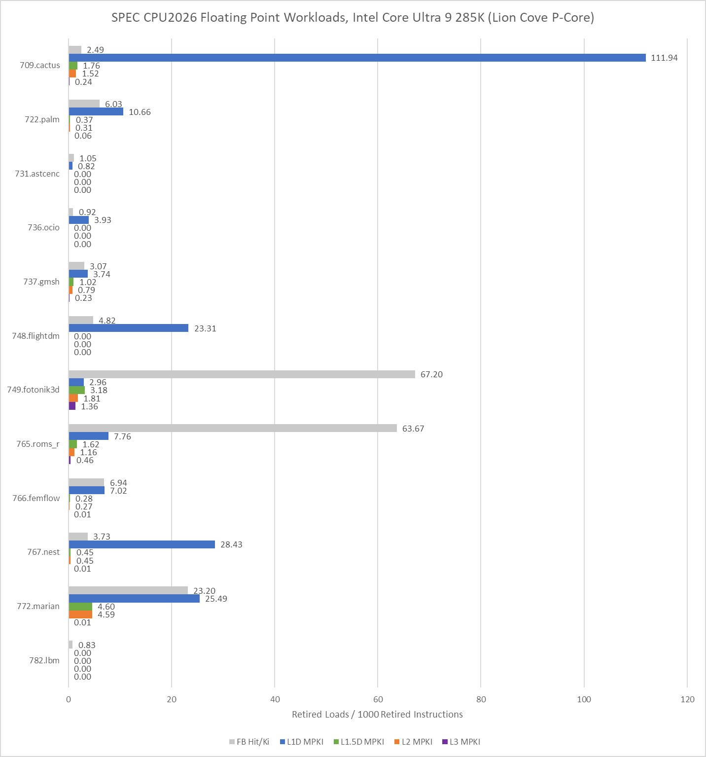
Intel’s performance counters can also account for Fill Buffer (FB) hits, which occur when a load asks for data from a cache line that already has an outstanding miss request. That can happen if data accesses have good spatial locality, and multiple instructions request data from the same cache line. FB hits can also happen if the prefetcher initiates a cache refill request before an instruction asks for it, but data hasn’t arrived yet when an instruction does make the request. I suspect 749.fotonik3d and 765.roms run into a combination of both. They have a lot of FB hits, but few instructions cause a fresh L3 miss. I suspect many instructions matched an existing miss request started by the prefetchers.
SPEC CPU2026 is a very different animal compared to its predecessor. The new suite has more variety on the code footprint side, with more tests that spill out of op caches and L1 instruction caches. On the other hand, branch prediction and data-side footprint have less variety. Few tests spill out of last level caches on AMD and Intel’s latest consumer chips, except for a couple of floating point workloads. I’m disappointed to see 520.omnetpp leave the room, because its behavior was the closest match across SPEC CPU2017 for gaming workloads.
Overall, those changes mean SPEC CPU2026 focuses more on core throughput than its predecessor. Larger instruction-side footprints do little to change that, because lowered branch prediction difficulties mean modern cores can smoothly stream code from their L2 caches. High IPC workloads certainly do exist, but it would have been nice if the newer suite improved coverage for lower IPC workloads too. Retaining an application like 520.omnetpp would have been nice. Instead, I feel like SPEC CPU2026 augments SPEC CPU2017’s coverage rather than being a perfect replacement.
2026-05-08 07:17:11
Applications vary wildly in what they demand from a system, making it difficult for a single benchmark to provide a broadly representative score. Benchmark suites try to address this by running a set of workloads that hopefully capture a range of typical application behavior. SPEC CPU2017 is an industry standard benchmark suite that dates back to 1989. Geekbench is another suite with a more recent history, going back to around 2010 if I remember correctly. Unlike SPEC CPU2017, Geekbench has a strong consumer focus. It’s distributed in binary form like most consumer applications, rather than source code form like SPEC CPU2017. Geekbench’s test harness and test runtimes also prioritize accessibility and ease of use.
Those differences make Geekbench 6 an interesting suite to evaluate alongside SPEC CPU2017. I looked at SPEC CPU2017 on Chips and Cheese several years ago. Now, I have a license for Geekbench 6 courtesy of Primate Labs’s founder, John Poole. It’s time to dig into the challenges Geekbench 6 workloads present for modern CPUs.
Because it’s distributed in binary form, Geekbench 6 can easily target ISA-specific features. Here, I’m running various workloads through Intel’s Software Development Emulator, which provides exact instruction counts and can emulate different ISA extensions without regard to what hardware it’s running on. With Intel’s Granite Rapids as an ISA target, AVX-512 plays a prominent role in Background Blur, Object Detection, and Structure from Motion. Granite Rapids represents Intel’s latest server platform, and comes with support for AMX for matrix multiplication acceleration. AMX shows up in Object Detection and Photo Library, where it accounts for 0.2% and 0.02% of executed instructions, respectively.
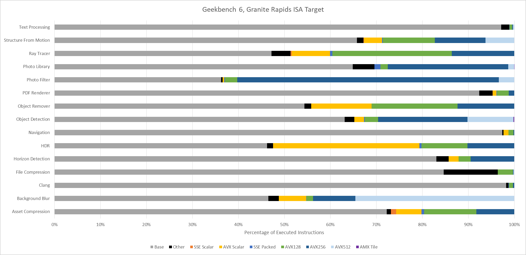
Even though AMX accounts for a small minority of executed instructions, AMX has an outsized impact. Ice Lake X represents an AVX-512 capable ISA target without AMX. Comparing results from Ice Lake X and Granite Rapids targets show that AMX can dramatically drop the number of AVX2 and AVX-512 instructions required to do the same work. Other tests show little to now difference between those two ISA targets, as expected.
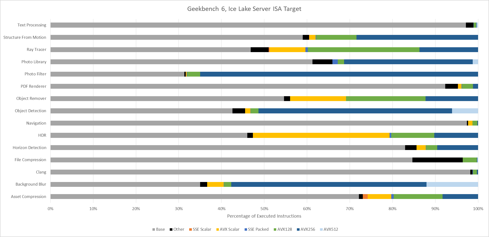
AVX(2) has a huge presence across Geekbench 6 workloads, to the point that it’s easier to name workloads that aren’t heavily vectorized than ones that are. Text Processing, File Compression, Clang, and PDF Renderer don’t have much vectorization. Everything else uses plenty of 128-bit or 256-bit vectors.
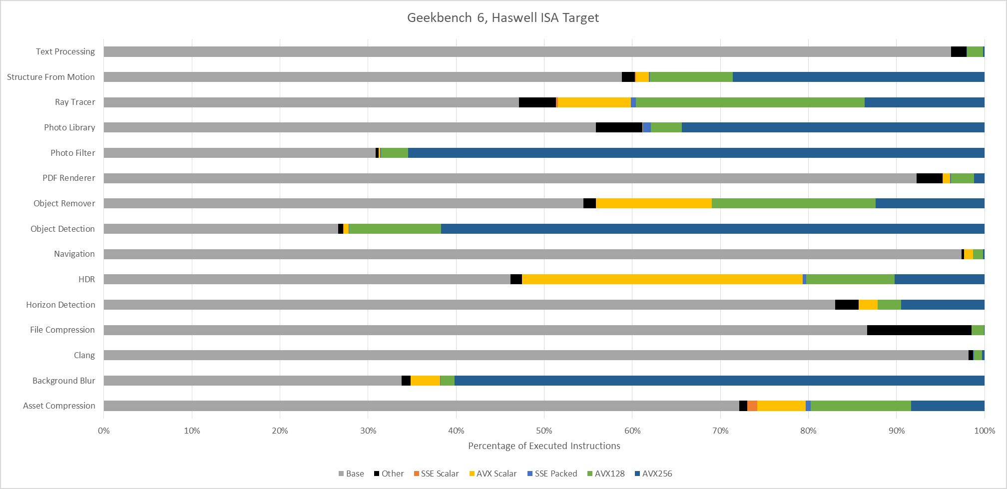
Moving to Haswell gives an AVX2 capable baseline with no AVX-512 support. The three heavy AVX-512 workloads see those AVX-512 instructions replaced by more AVX2 ones. Object Detection is a particularly prominent example, with 256-bit AVX2 dominating the instruction stream.
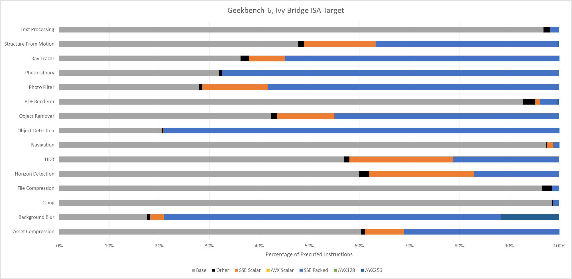
An Ivy Bridge ISA target gives an idea of what happens with AVX support, but not AVX2. AVX provides 256-bit vector registers and 256-bit load/store operations, but 256-bit vector math operations are limited to floating point. With SDE emulating an Ivy Bridge ISA target, the executed instruction stream skews heavily towards 128-bit packed SSE operations. 256-bit AVX still shows up in many workloads, but accounts for less than 1% of executed instructions across most of them. Only Background Blur makes heavy use of 256-bit AVX.
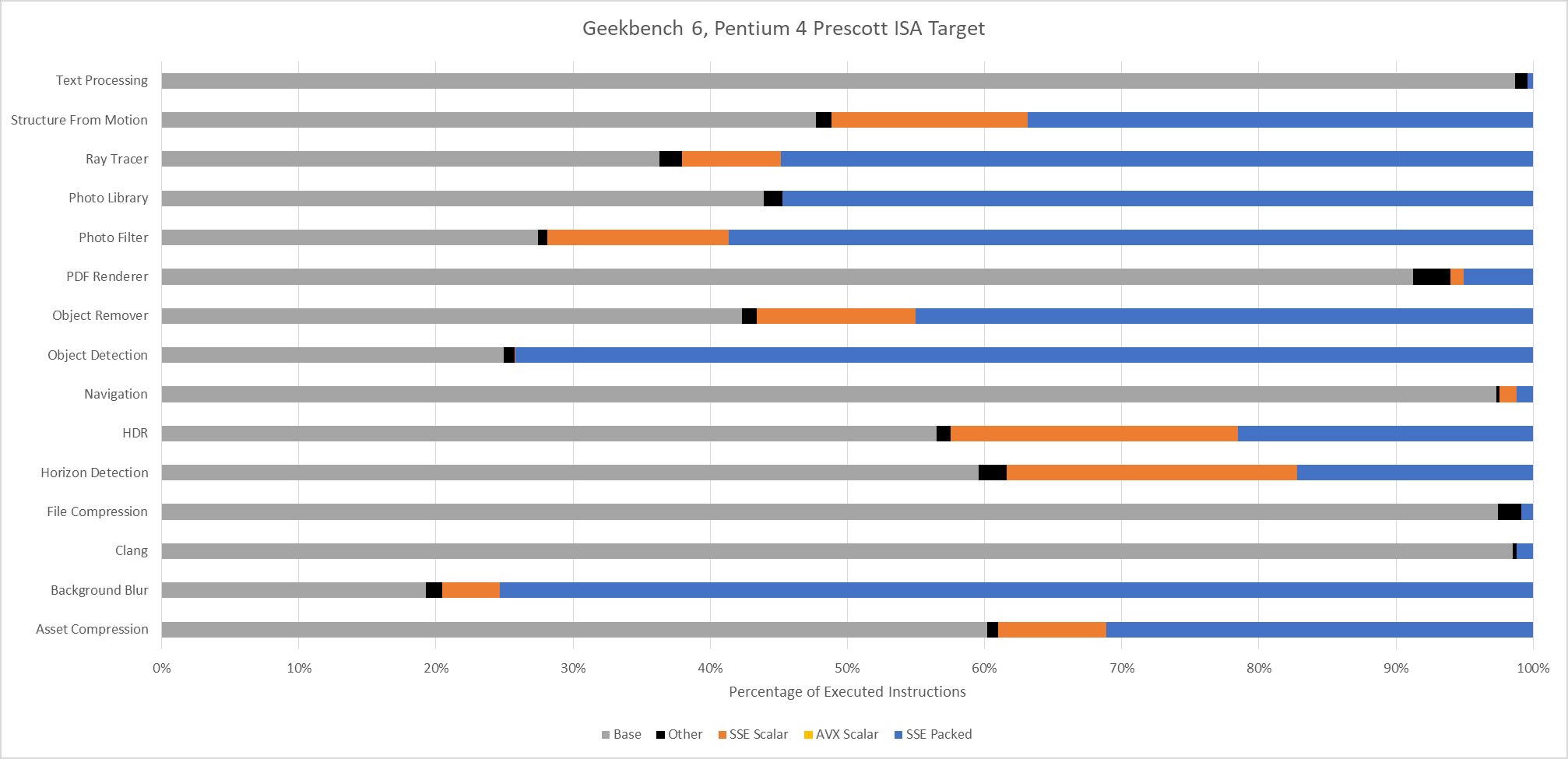
Lastly, Intel’s Pentium 4 “Prescott” represents an x86-64 baseline from long ago. It’s mostly here for curiosity, as there are likely very few systems in service limited to this level of ISA extension support. The executed instruction distribution is surprisingly close to that of Ivy Bridge. 128-bit packed SSE operations dominate across most workloads.
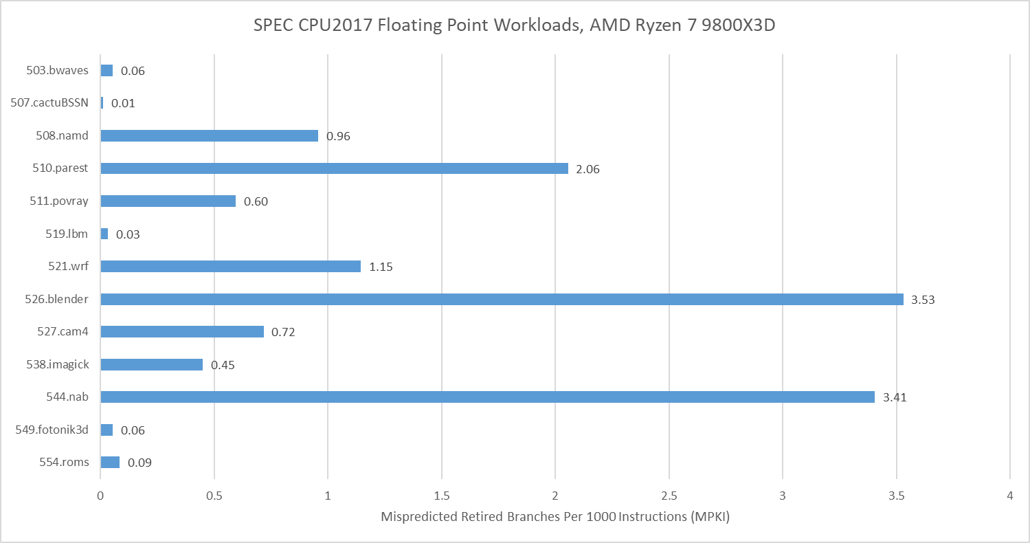
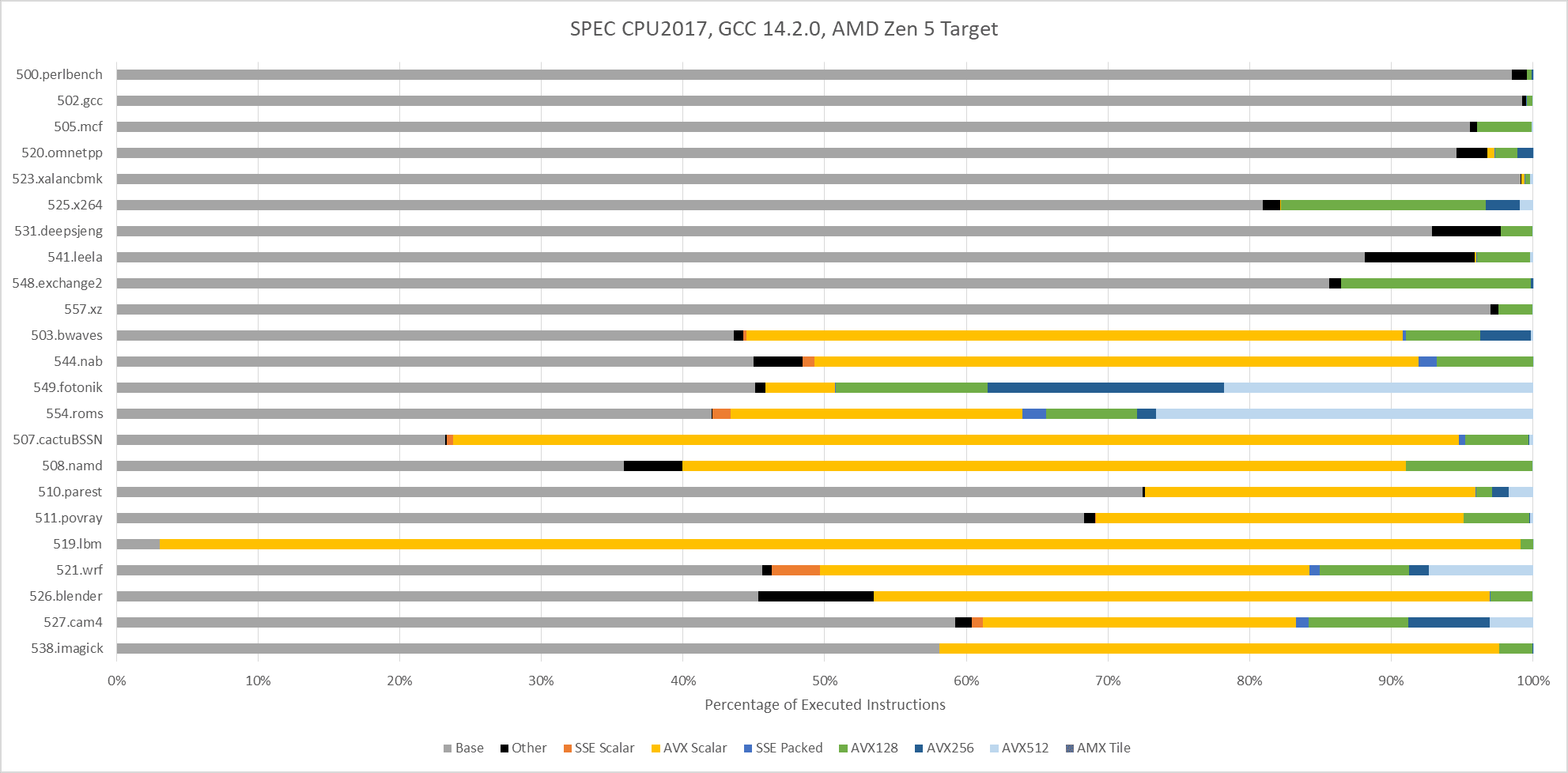
SPEC CPU2017 doesn’t explicitly target ISA features, including vector extensions. To maximize portability, SPEC CPU relies on compilers to find opportunities to use ISA features. With GCC 14.2.0 compiling for an AVX-512 capable target (Zen 5), vector ISA extensions do show up in a few floating point tests. 549.fotonik3d and 554.roms execute a lot of AVX-512 instructions. Elsewhere, auto-vectorization plays a comparatively minor role. It’s almost absent in SPEC CPU2017’s integer suite, except in 525.x264 and 548.exchange2. Those two workloads use some 128-bit vectors.
Instructions per cycle gives a quick overview of how “difficult” a workload is, for lack of a better word. Low IPC often indicates a workload is bound by branch mispredicts or cache misses, or less often, by hitting a particular deficiency in the core. Games for example tend to be low IPC workloads, bound primarily by the memory subsystem. High IPC in contrast points to a well fed core, with focus shifting to how fast the core can crunch through instructions.
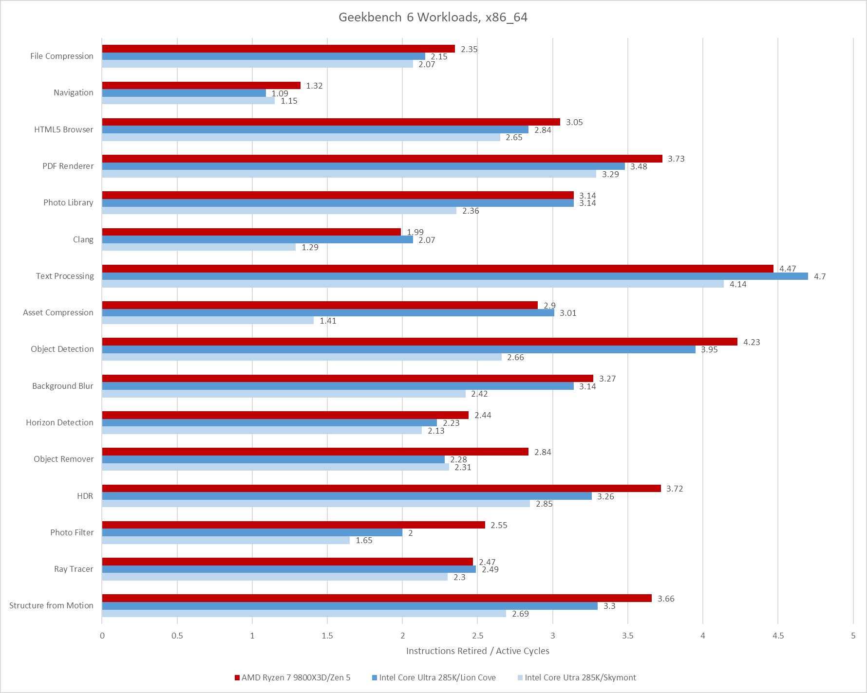
Geekbench 6’s IPC distribution is skewed towards the medium to medium-high IPC range. Many workloads average well beyond 2 IPC on high performance cores like Intel’s Lion Cove and AMD’s Zen 5. Skymont isn’t explicitly a high performance core, but can often get close in IPC terms. However, it’s more prone to “glass jaw” cases, as can be seen in Clang, Asset Compression, Photo Library, and Structure From Motion.
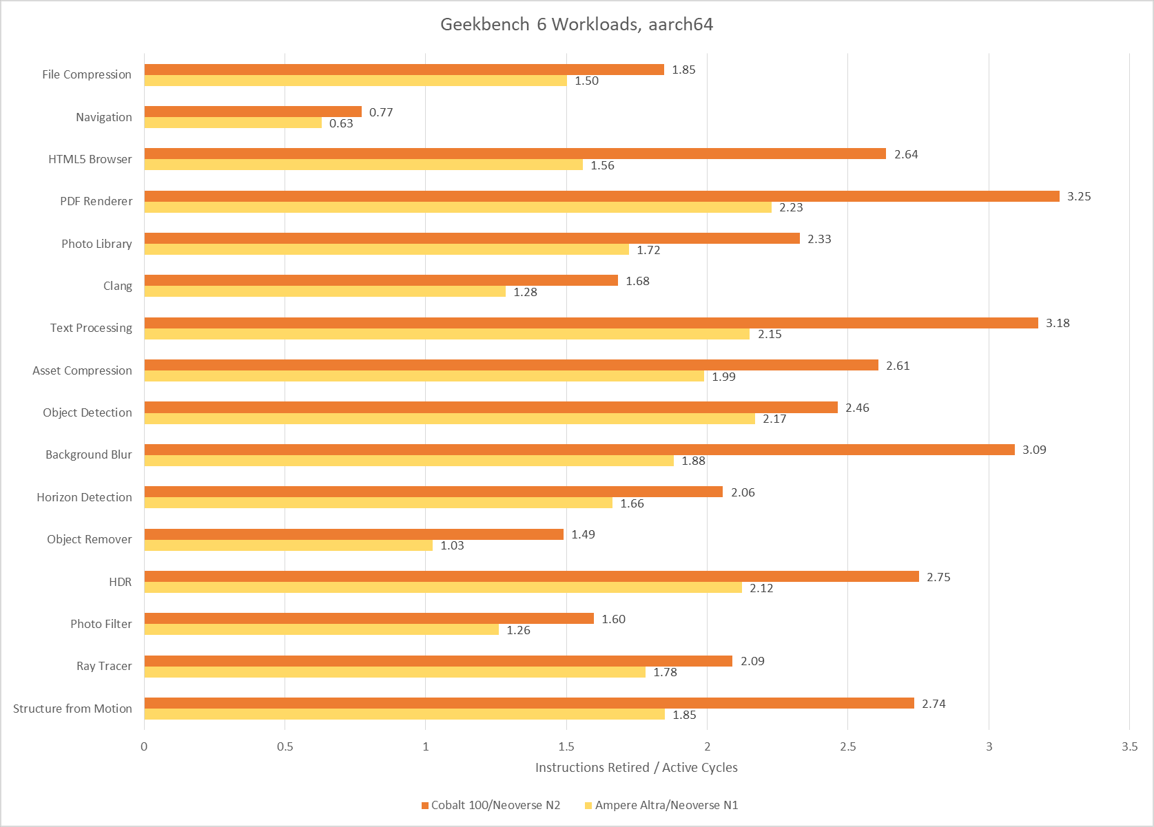
Poking around with a couple of aarch64 cores tells much the same story. Arm’s Neoverse N1 and Neoverse N2 achieve reasonably good throughput considering their likely design targets. I consider anything above 2 IPC to be high for a 4-wide core, and Neoverse N1 hits plenty of those cases. Neoverse N2 is a 5-wide core ,and sails past 3 IPC on several tests. Neoverse N1 does end up with somewhat low IPC on Object Remover, but I suspect that’s down to a weaker vector execution setup. Only Navigation sticks out as a persistently difficult, low IPC workload across all the CPUs I tested.
SPEC CPU2017 shows a wider IPC distribution, with more difficult low IPC workloads. That’s especially the case for SPEC’s integer suite, where 505.mcf and 520.omnetpp pose huge challenges even for sophisticated, high performance cores.
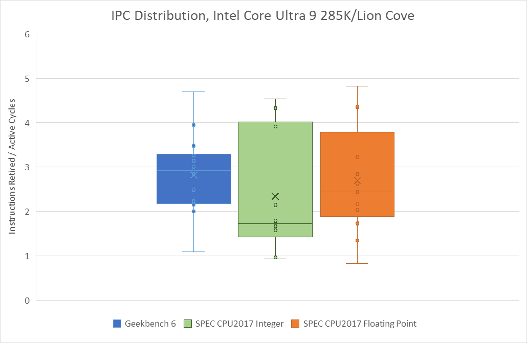
Geekbench 6’s IPC distribution lands closer to that of SPEC’s floating point suite, though SPEC still shows more IPC variation. 549.fotonik3d is a very low IPC outlier, and represents a corner case bound by how much bandwidth a single core can pull from DRAM. In general, Geekbench 6 has a much tighter IPC distribution across its workloads than SPEC does.
Branch prediction is both difficult and vital to high performance. Modern cores devote enormous resources to branch prediction. Geekbench 6 has several workloads that challenge branch predictors even on modern cores.
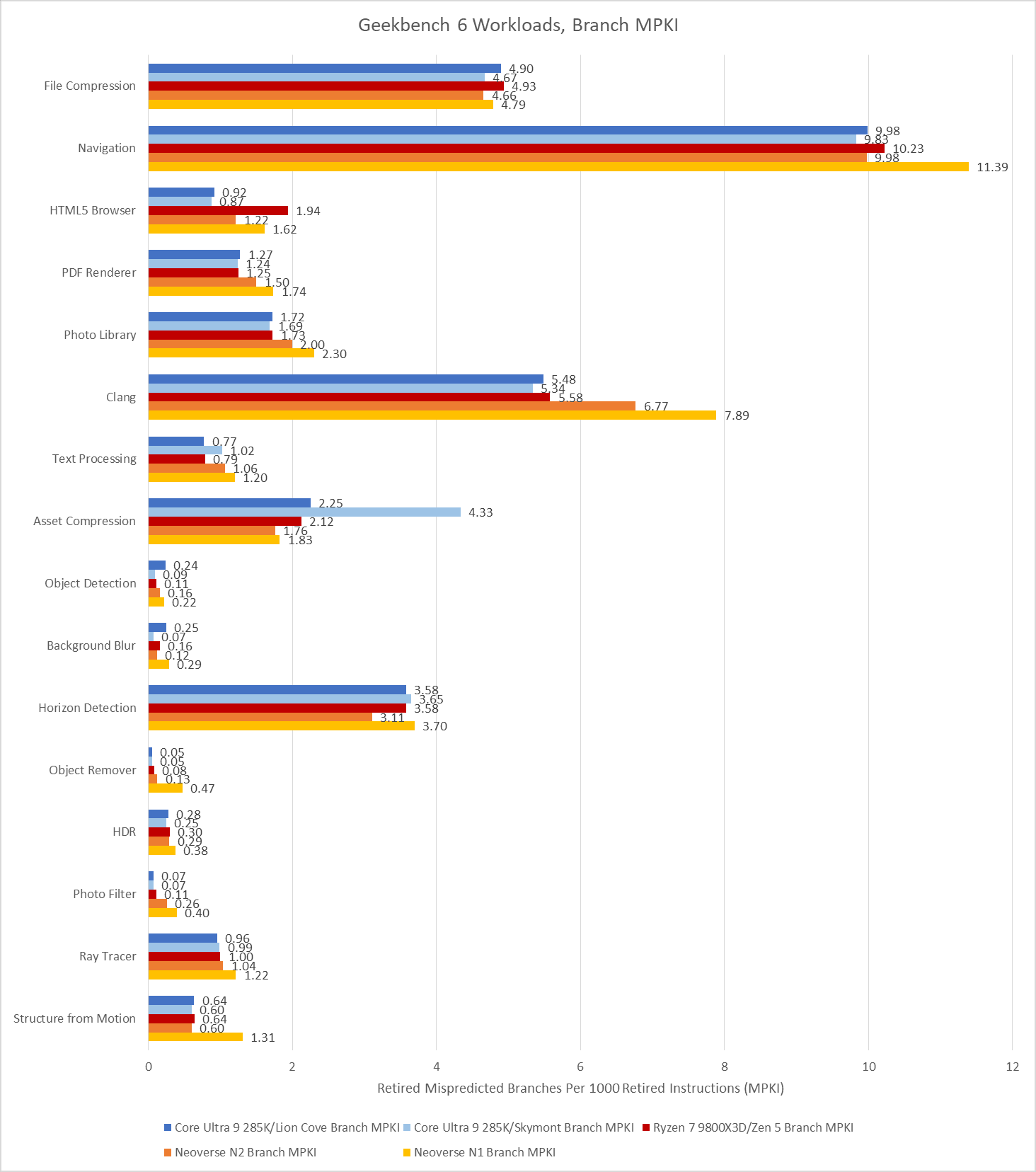
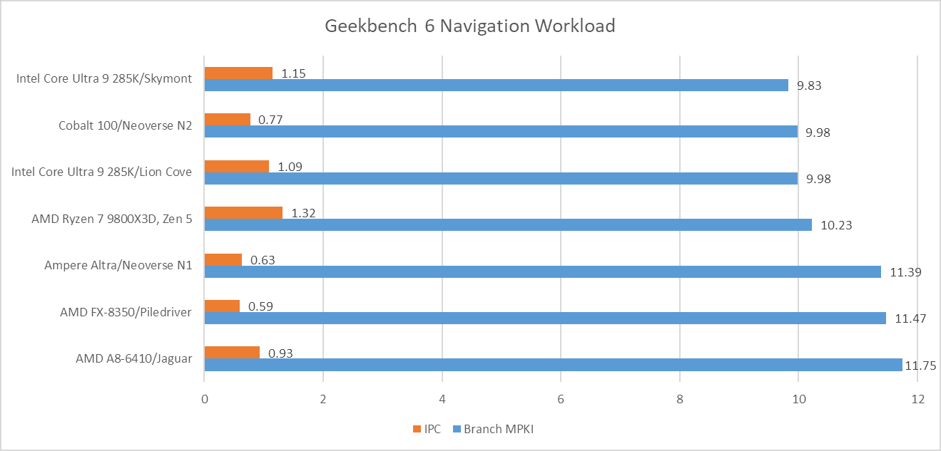
Navigation is by far the worst, with a high enough MPKI figure that mispredicts are likely the single biggest reason behind its low IPC. More advanced predictors help, but don’t solve the problem. That creates a curious situation where newer cores see little IPC improvement compared to older, smaller ones from over a decade ago.
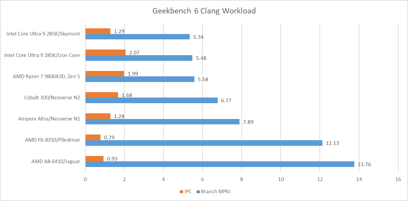
Aside from Navigation, File Compression and Clang present moderate challenges for branch predictors. Newer predictors tend to help in Clang, while older ones tend to get shredded.
Asset Compression is an interesting case, because branch prediction normally isn’t a problem in that workload. MPKI is well under control on Lion Cove, Zen 5, and both Neoverse cores. Even much older predictors with less storage budget and less advanced prediction techniques do reasonably well. Piledriver gets away with 2.76 MPKI, while Jaguar is just a tad worse at 2.96 MPKI. However, Skymont’s normally competent predictor trips over itself in this workload suffering 4.33 branch MPKI.
Cache misses can be another major challenge for modern CPUs. On the instruction side, only Clang has a large enough code footprint to spill out of Lion Cove’s 5.2k entry op cache. On the other end of the spectrum, several Geekbench 6 workloads appear to spend much of their time executing tiny loops. In PDF Renderer, HDR, and Photo Filter, Lion Cove’s frontend is often able to feed the core out of its 192 entry loop buffer. That doesn’t improve core throughput because Lion Cove is still limited by its 8-wide rename and allocate stage downstream, but it does suggest excellent code locality in those workloads. High loop buffer usage can also help save power, because much of the frontend could be turned off when running code out of the loop buffer.
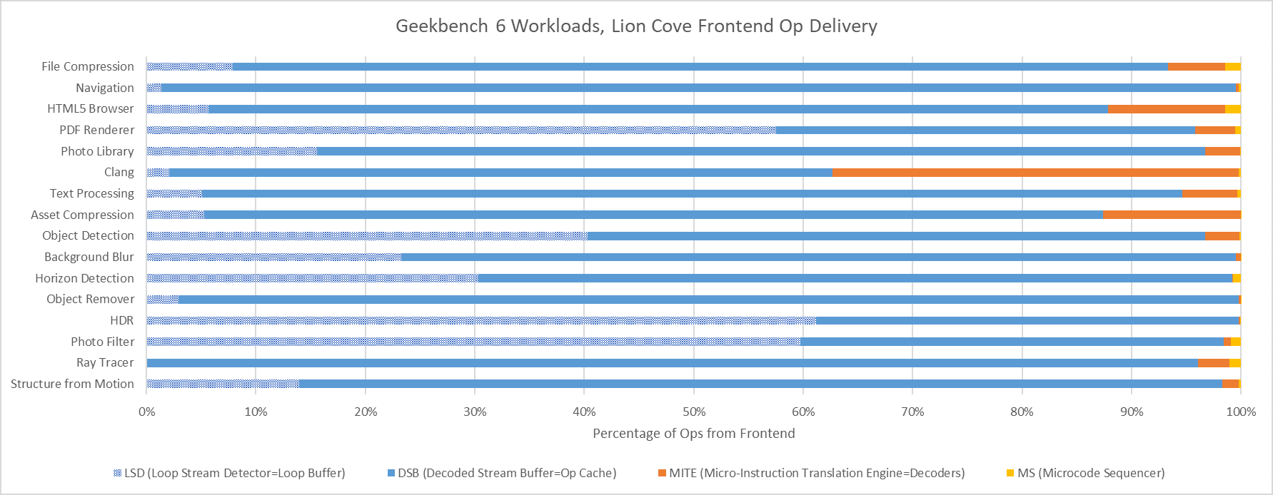
Zen 5 has an even larger op cache with 6K entries, and a well optimized one at that. Again, Clang is the only workload that offers any significant challenge to the op cache. Even then, Zen 5 can mostly feed itself from the op cache rather than the decoders. That’s very much where AMD wants to be, since Zen 5’s decoder setup is weaker than Lion Cove’s when running a single thread.
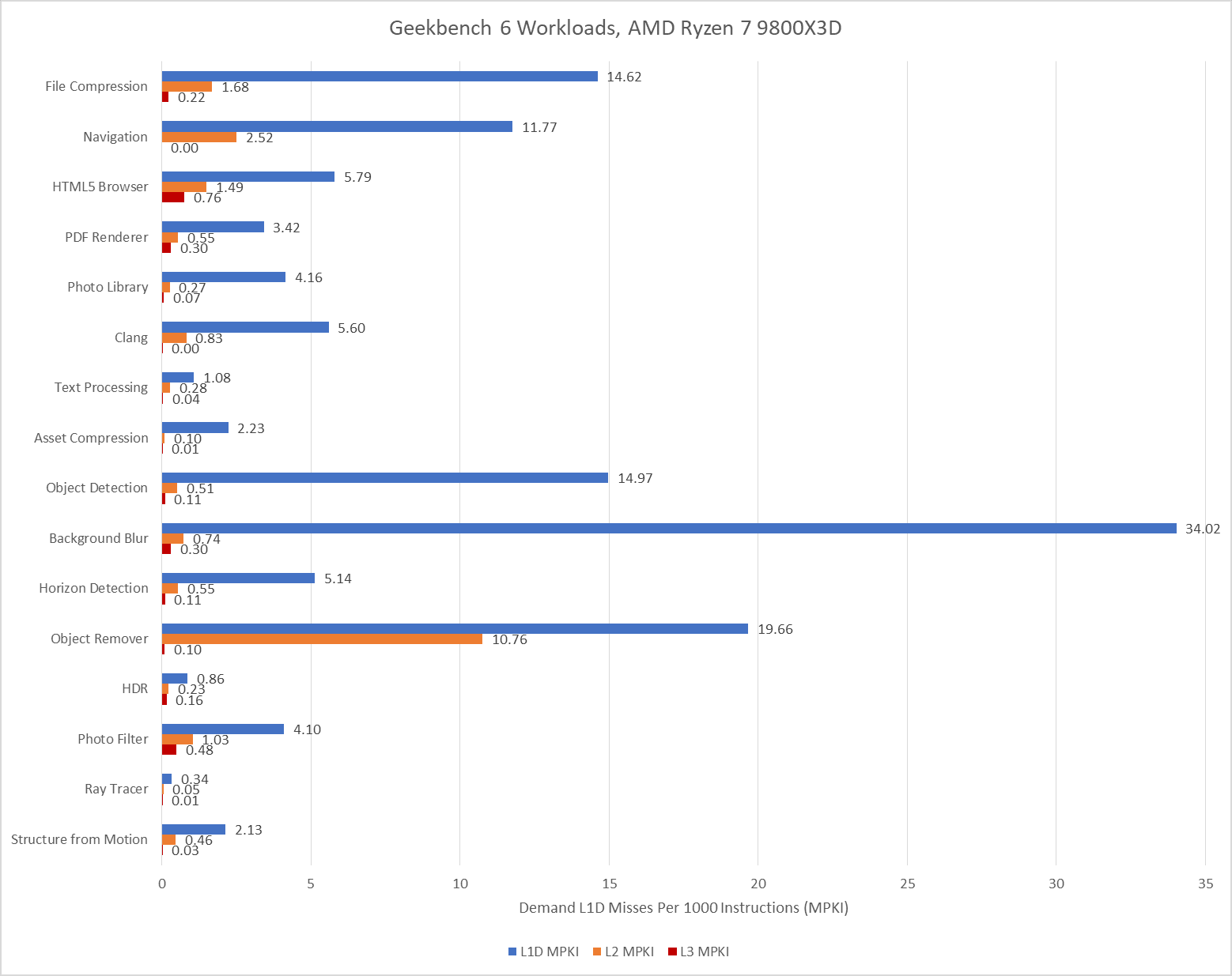
Data-side memory accesses tend to have more challenging patterns. Many of Geekbench 6’s workloads create heavy L1D miss traffic on Lion Cove. Most of these L1D misses are caught at L2. Lion Cove’s large 3 MB L2 pulls a lot of weight in making sure the core can sustain high IPC across much of Geekbench 6’s suite, despite high L3 latency. The new 192 KB L1.5D cache does well to, and occasionally captures the vast majority of L1D misses. Object Remover stands out as the only test with very high L2 miss traffic on Lion Cove.
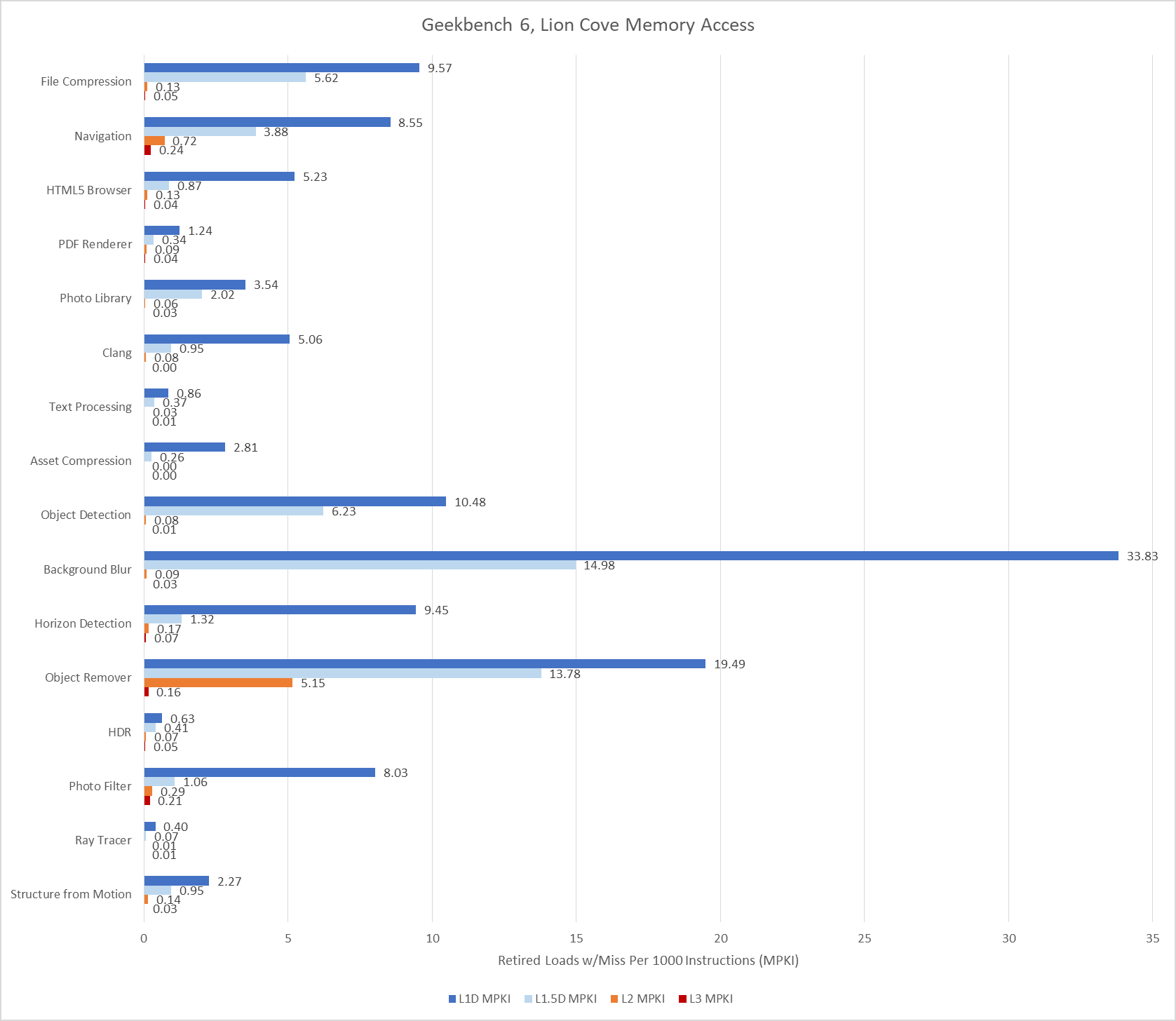
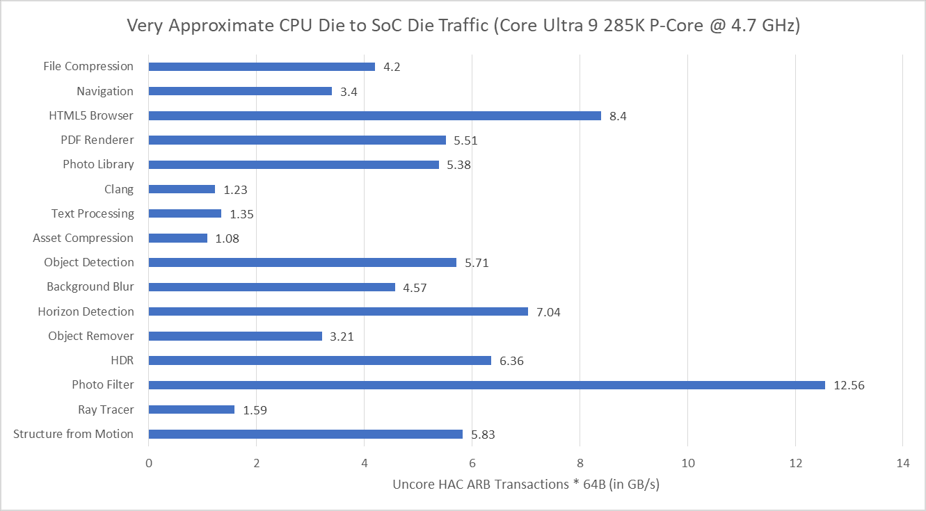
L3 misses tend to be low, hinting at good data locality or predictable access patterns. Performance counters here specifically count the first retired load that created a miss to a 64B line. If a load requests data from a cache line that already has a miss request in progress, initiated either by a previous load or a prefetch, that counts as a FB (fill buffer) hit. I didn’t log that here. However, I did track traffic right in front of the CPU tile’s die-to-die interface, at what Intel calls the arbitration queue. I’m using that as a proxy for CPU-side L3 miss and DRAM bandwidth.
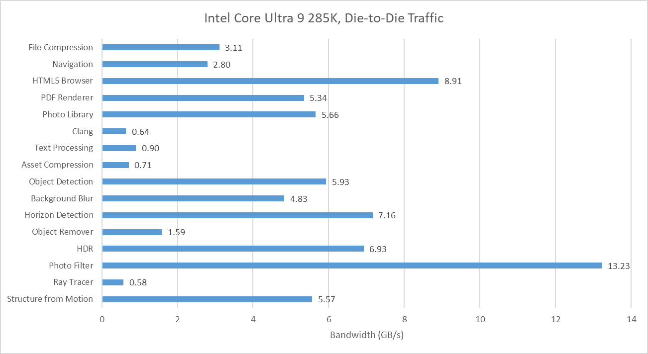
Many of Geekbench 6’s workloads request multiple gigabytes per second across the die-to-die interface, though none push the memory subsystem from a single thread as hard as SPEC CPU2017’s fotonik3d. Photo Filter is the most bandwidth heavy test in Geekbench 6, despite having a tame-looking 0.23 L3 MPKI figure. That suggests Lion Cove’s prefetcher is able to initiate many memory requests before an instruction asks for the data. Prefetching helps mitigate DRAM latency and keep IPC up. That low MPKI figure contrasts with behavior in games, which tend to miss L3 and can be sensitive to DRAM latency.
AMD’s performance events count demand data cache refills, rather than tagging loads with data sources and counting at retirement. Demand means a refill initiated by an instruction, as opposed to the prefetcher. They’ll generally give higher counts compared to events at retirement, especially if a lot of instructions execute but are later flushed (for example from branch mispredicts).
With 96 MB of L3, the Ryzen 7 9800X3D practically eliminates L3 misses for the Navigation workload and improves in Object Remover too. Elsewhere, the difference in where events are counted and the low L3 miss activity overall makes it hard to tell if the larger cache helps compared to the 36 MB L3 in Arrow Lake. Further up in the memory subsystem, Zen 5’s smaller 1 MB L2 can still be very effective, but often suffers more misses than Lion Cove’s larger L2. AMD has to rely a little more on their L3, which does have better performance than Intel’s.
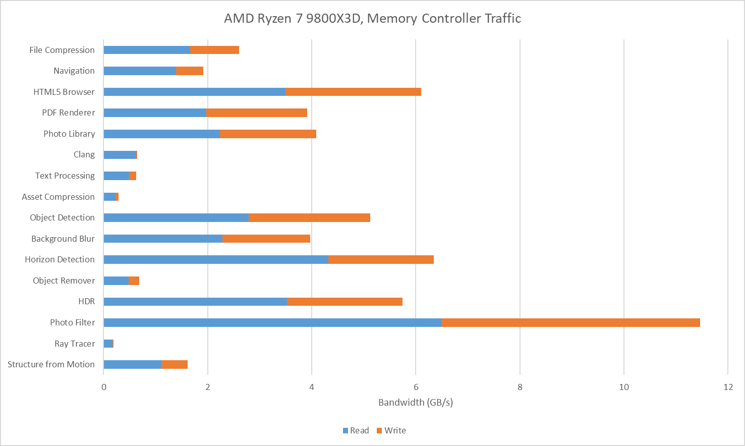
I also tracked traffic at the Ryzen 7 9800X3D’s memory controllers. I tried to gather data at the IO die side of the die-to-die interface (CCMs), but couldn’t get Data Fabric performance events figured out for write traffic. Unified Memory Controller (UMC) data should be adequate anyway because I have the iGPU disabled and should have very little IO traffic while running Geekbench 6 workloads. The Ryzen 7 9800X3D overall has lower DRAM traffic than on the 285K, likely thanks to the former’s larger L3. Generally though, the pattern is similar. Photo Filter stands out as a bandwidth heavy but prefetch friendly workload. HTML5 Browser and Horizon Detection slot into the same category.
Both Geekbench 6 and SPEC CPU2017 scores are given in speedup relative to a reference system. Geekbench 6’s reference system is a Dell Precision 3460 with a Core i7-12700, which is set to a baseline score of 2500. SPEC CPU2017’s reference system is a Sun Fire V490 with 2.1 GHz UltraSPARC-IV+ processors, which is set to a score of 1.
I find SPEC CPU2017’s score easier to interpret because it’s simply a speedup ratio, while Geekbench 6’s score takes a bit more math to get there. On the flip side, Geekbench 6’s reference system is more modern and relevant. The Sun Fire V490 dates back to 2009, and already performed poorly compared to systems from just a few years later. A Sandy Bridge or Bulldozer system would provide a far better reference point.
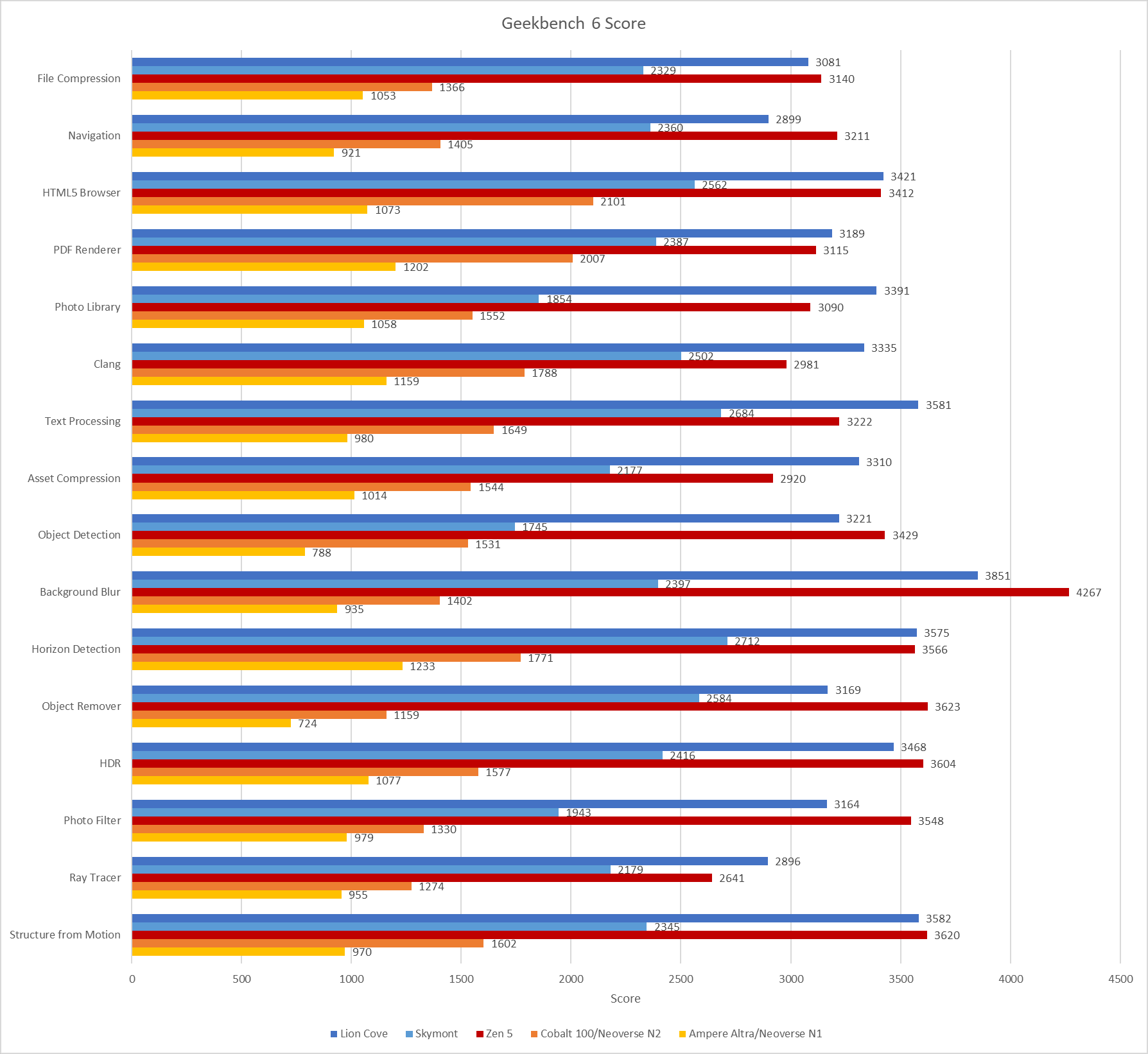
Geekbench 6’s reference system also has strong vector execution capabilities, assuming the workloads mostly ran on the 12700’s P-Cores. Geekbench 6’s workloads tend to be vector heavy, so the baseline sets rather demanding expectations. Skymont has weak vector execution despite improving on prior E-Cores, and often falls below the 2500 score baseline. The same applies to Arm’s Neoverse N1 and N2, though those cores also fall behind because they’re optimized for lower performance targets in general.
Geekbench 6 is a vector-heavy suite that emphasizes core throughput. Many workloads have small instruction footprints, enjoy good branch prediction accuracy, and are prefetcher friendly. There are exceptions of course. Navigation stands out as one of the only low IPC workloads, bound by branch mispredicts. Clang does run into some op cache misses, though the larger op cache on Zen 5 still does very well, and other factors seem to hold back its IPC before Zen 5’s per-thread, 4-wide decoders present a limitation.
SPEC CPU2017 shows some of the same characteristics, with a large number of workloads that don’t pressure the memory subsystem as much as games do. While SPEC captures a broader range of IPC-related challenges, its emphasis on portability means it doesn’t stress vector execution as much as Geekbench 6 can. Both suites ultimately serve different purposes, and neither can be used in place of the other. Going forward, I expect both SPEC and Primate Labs to continue evaluating application behavior, and update their workloads as typical application behavior evolves.
2026-04-08 12:29:08
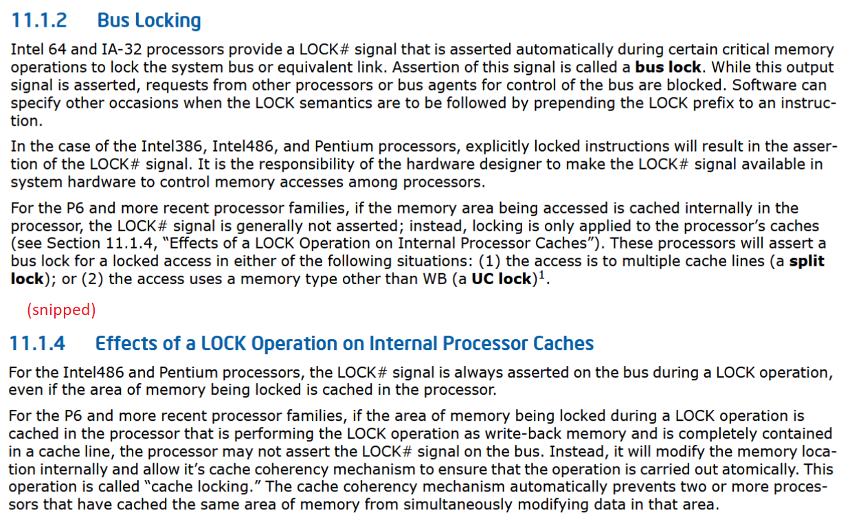
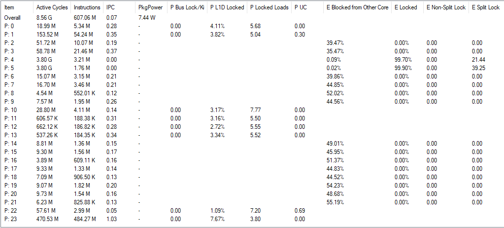
“Split locks” are atomic operations that access memory across cache line boundaries. Atomic operations let programmers perform several basic operations in sequence without interference from another thread. That makes atomic operations useful for multithreaded code. For instance, an atomic test and set can let a thread acquire a higher level lock. Or, an atomic add can let multiple threads increment a shared counter without using a software-orchestrated lock. Modern CPUs handle atomics with cache coherency protocols, letting cores lock individual cache lines while letting unrelated memory accesses proceed. Intel and AMD apparently don’t have a way to lock two cache lines at once, and fall back to a "bus lock" if an atomic operation works on a value that’s split across two cache lines.
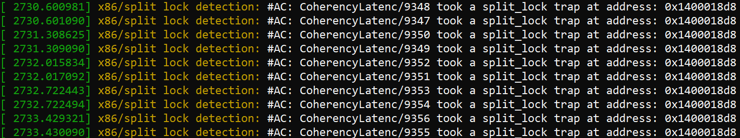
Bus locks are problematic because they’re slow, and taking a bus lock “potentially disrupts performance on other cores and brings the whole system to its knees”. AMD and Intel’s newer cores can trap split locks, letting the kernel easily detect processes that use split locks and potentially mitigate that noisy neighbor effect. Linux defaults to using this feature and inserting an artificial delay to mitigate the performance impact.
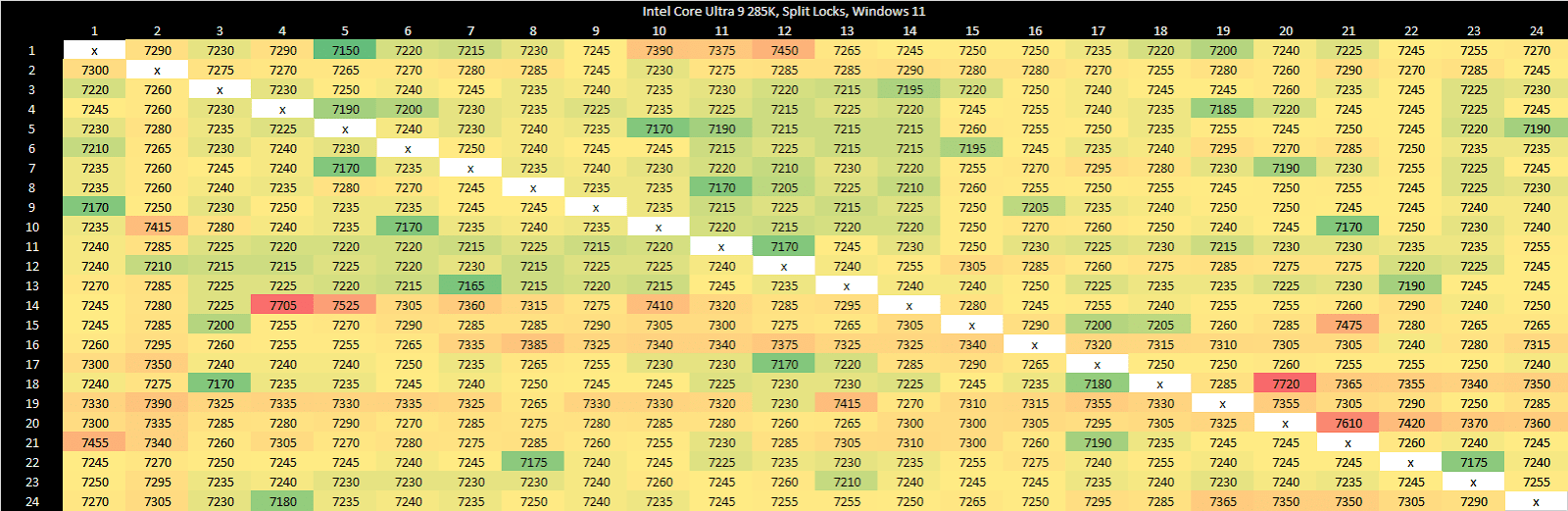
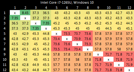
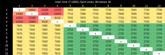
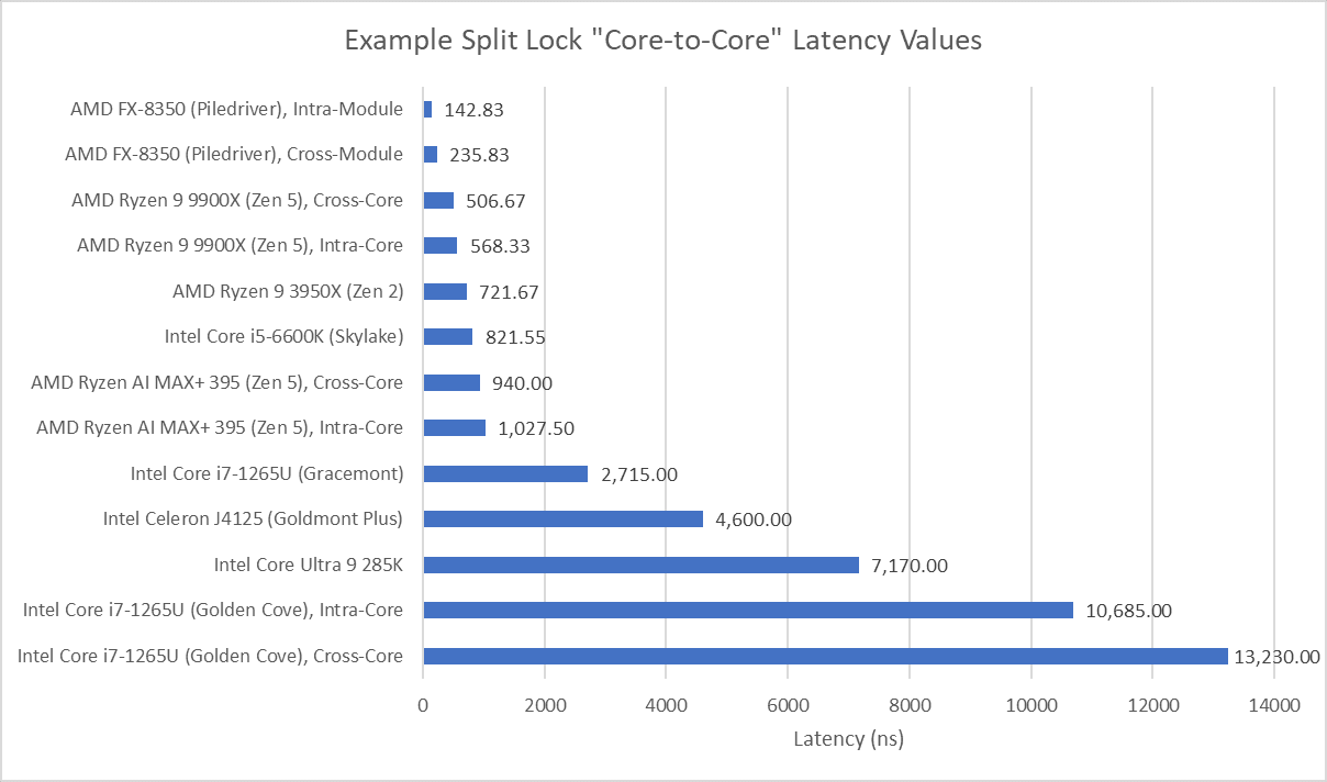
I have a core to core latency test that bounces an incrementing counter between cores using _InterlockedCompareExchange64. That compiles to lock cmpxchg on x86-64, which is an atomic test and set operation. I normally target a value at the start of a 64B aligned block of memory, but here I’m modifying it to push the targeted value’s start address to just before the end of the cache line. Doing so places some bytes of the targeted 8B (64-bit) value on the first cache line, and the rest on the next one. As expected, “core to core latency” with split locks range from bad to horrifying.
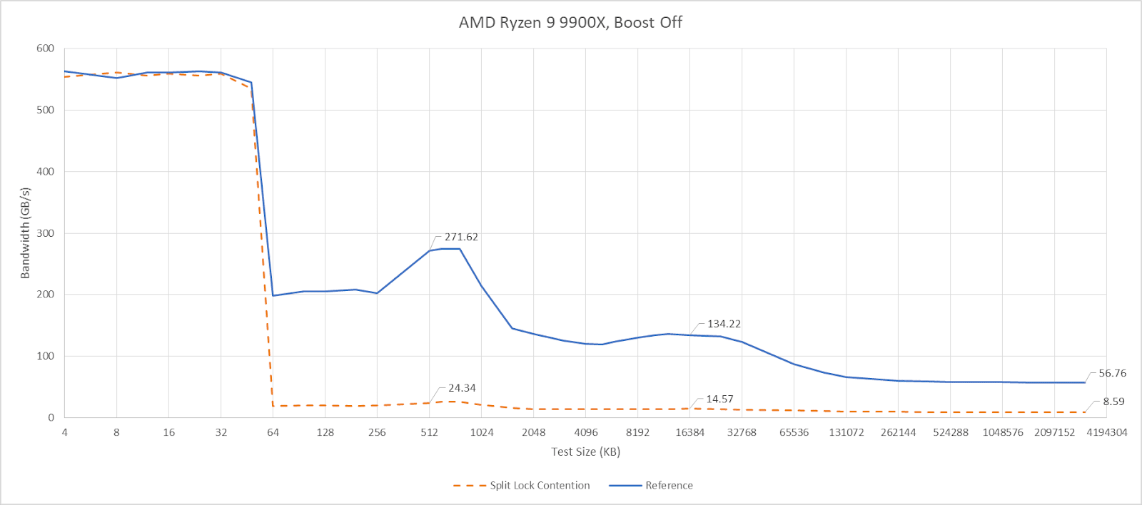
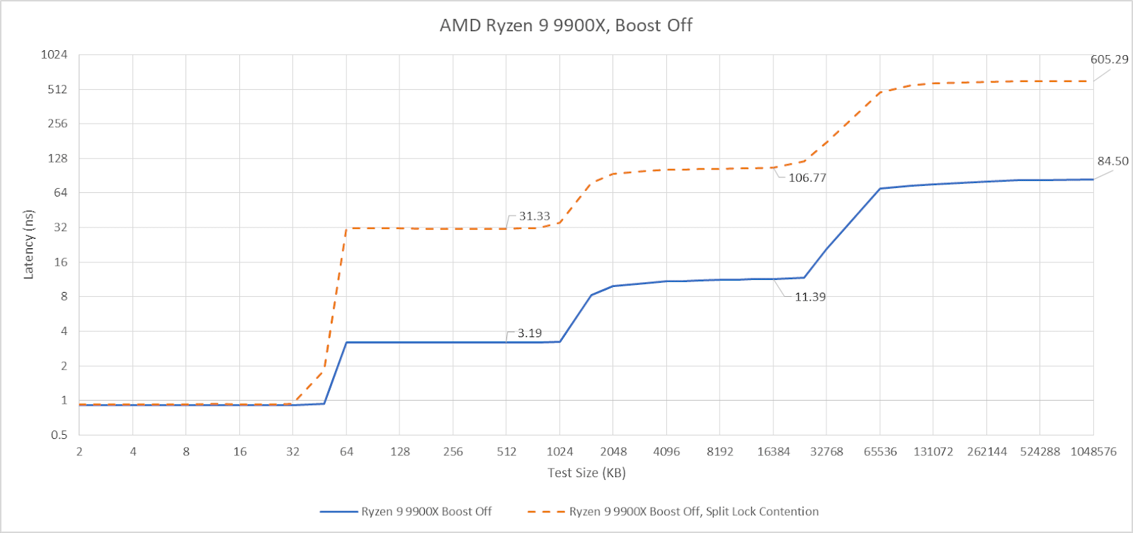
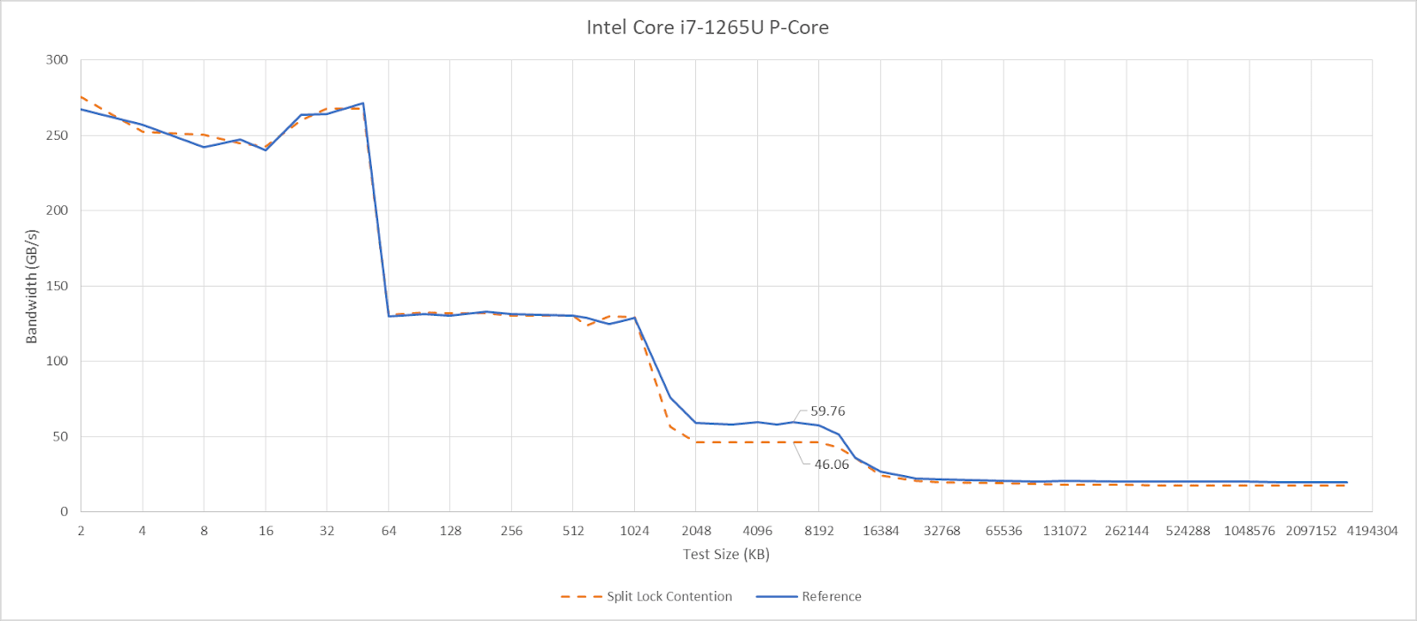
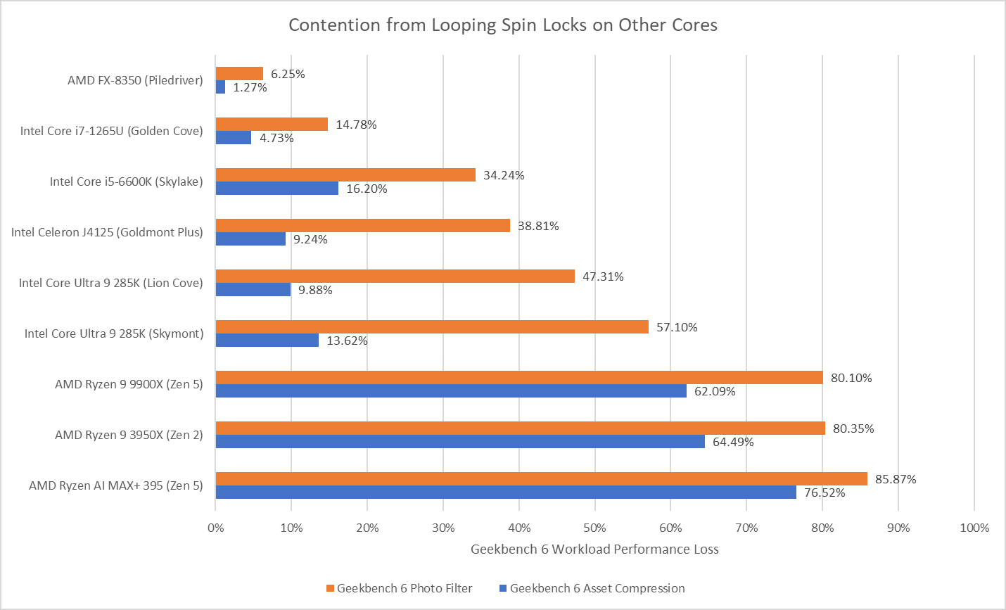
To assess the potential disruption from split locks, I ran memory latency and bandwidth microbenchmarks on cores excluded from the core to core latency test. Besides microbenchmarks, I ran Geekbench 6’s photo filter and asset compression workloads. The photo filter workload generates a lot of cache miss traffic, while asset compression tends to be the opposite. Many recent CPUs only achieve their highest clock speeds with two or fewer cores active. One core will be loaded by the workload being tested for contention effects, and another pair will be used for the core to core latency test. I therefore turned off boost or lowered clock speeds on some of the tested hardware to reduce noisy neighbor effects from clock speed variation, helping isolate the effects of split locks.
Intel’s Arrow Lake gets to be the first victim. Normal core to core latency results look like this:
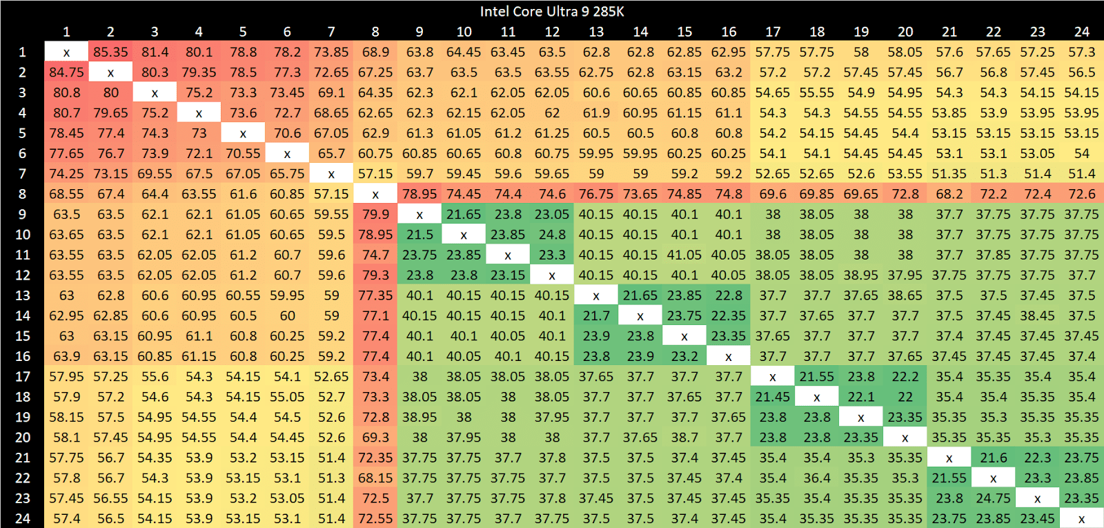
Split locks send latency to 7 microseconds, which remains mostly constant across different core types.
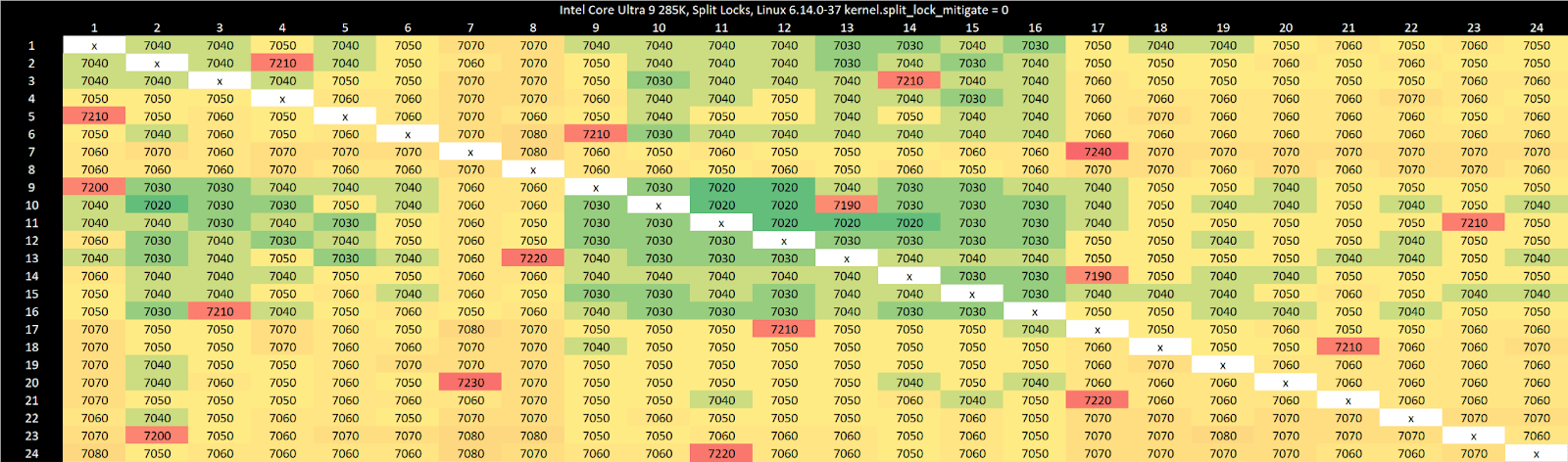
On Arrow Lake, split locks only affect L2 misses. It’s close to a “bus lock” in the traditional sense because it affects the first level in the memory hierarchy shared by all CPU cores. In theory a program can be completely unaffected by split locks as long as it keeps hitting in L2 or faster caches.
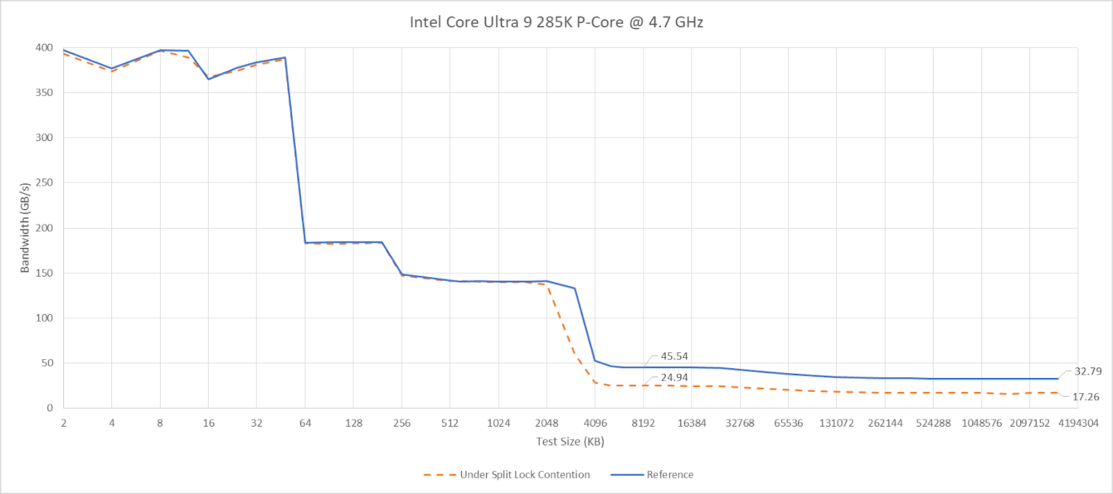
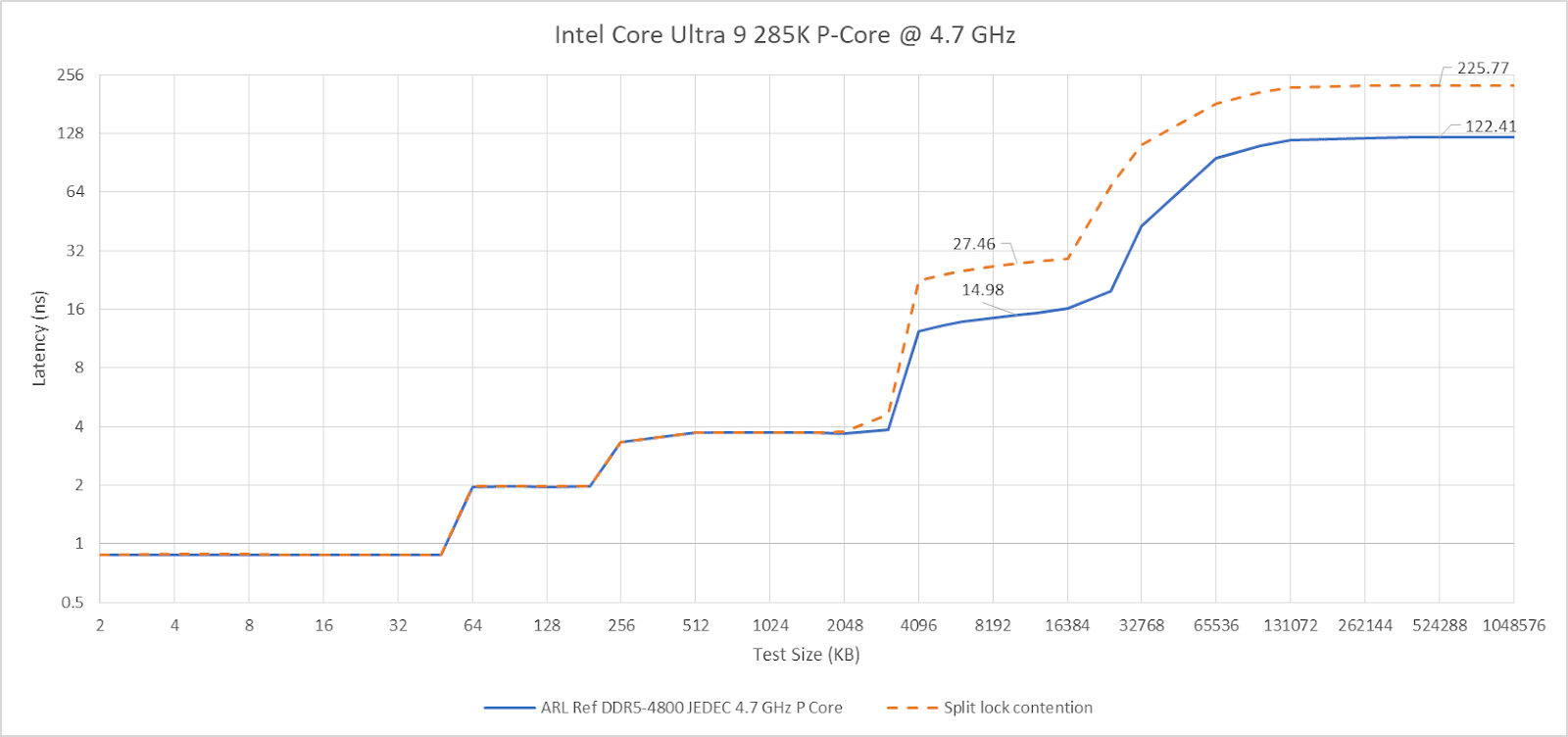
Past L2, split lock contention roughly halves memory access performance. Curiously, the 4 MB L2 caches shared across quad-core E-Core clusters aren’t affected, even if split locks are being looped from a pair of cores within the same cluster.
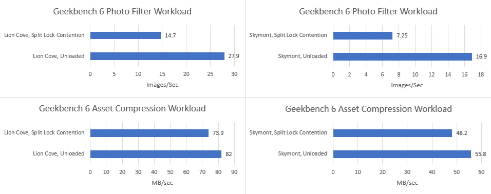
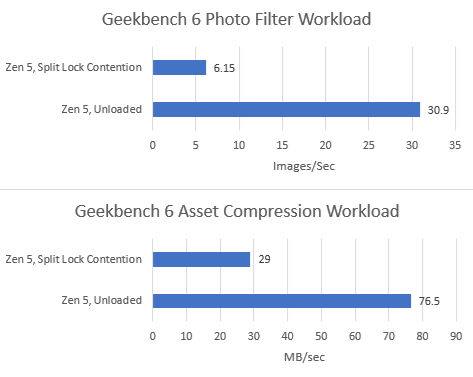
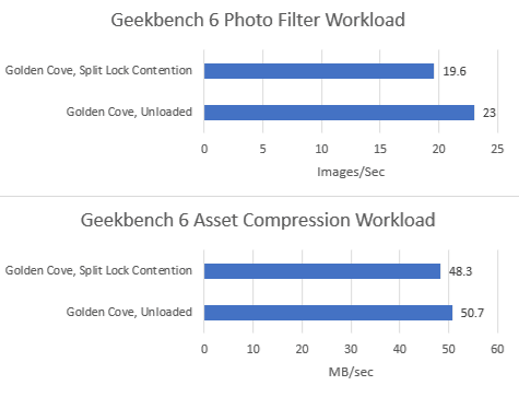
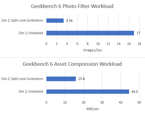
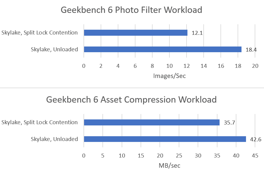
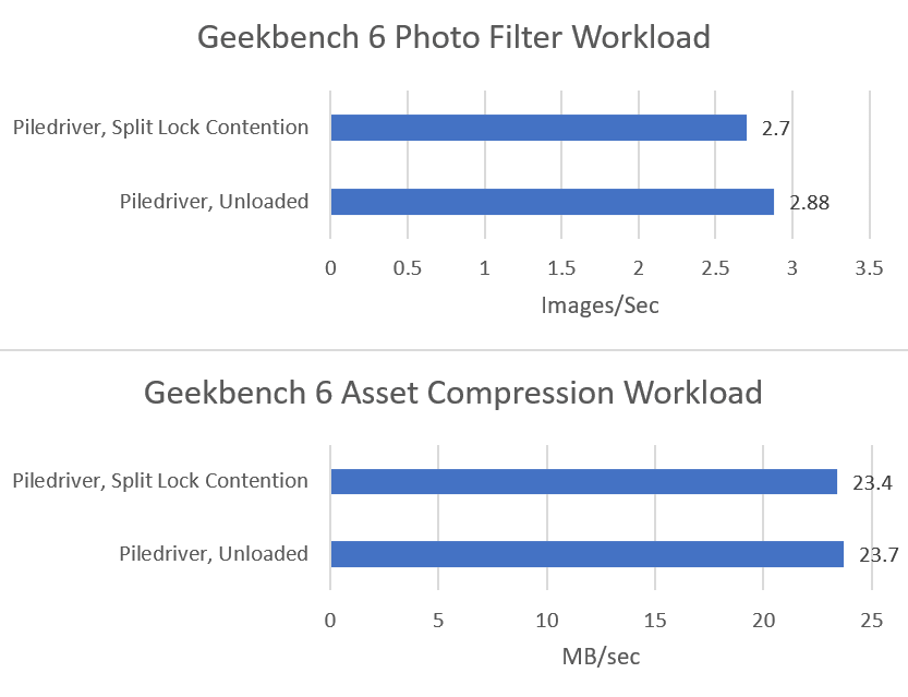
Split locks heavily impact GB6’s photo filter workload. Asset compression also takes a hit, but gets away relatively unscathed.
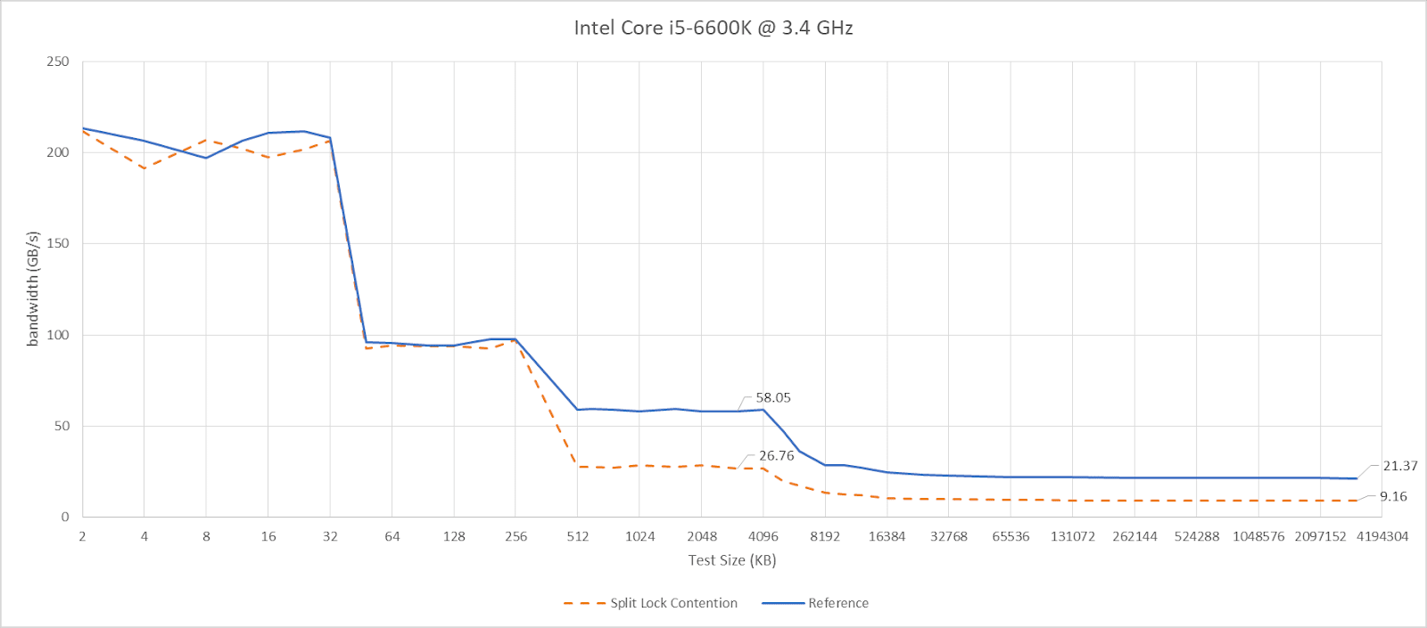
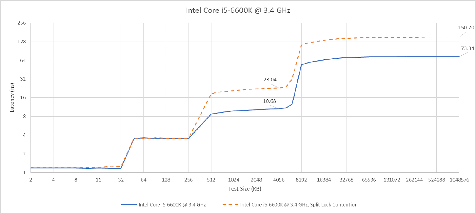
Zen 5 has better split lock latency than Arrow Lake, though 500 ns is still bad in an absolute sense. As on Arrow Lake, core cluster boundaries don’t affect split lock performance.
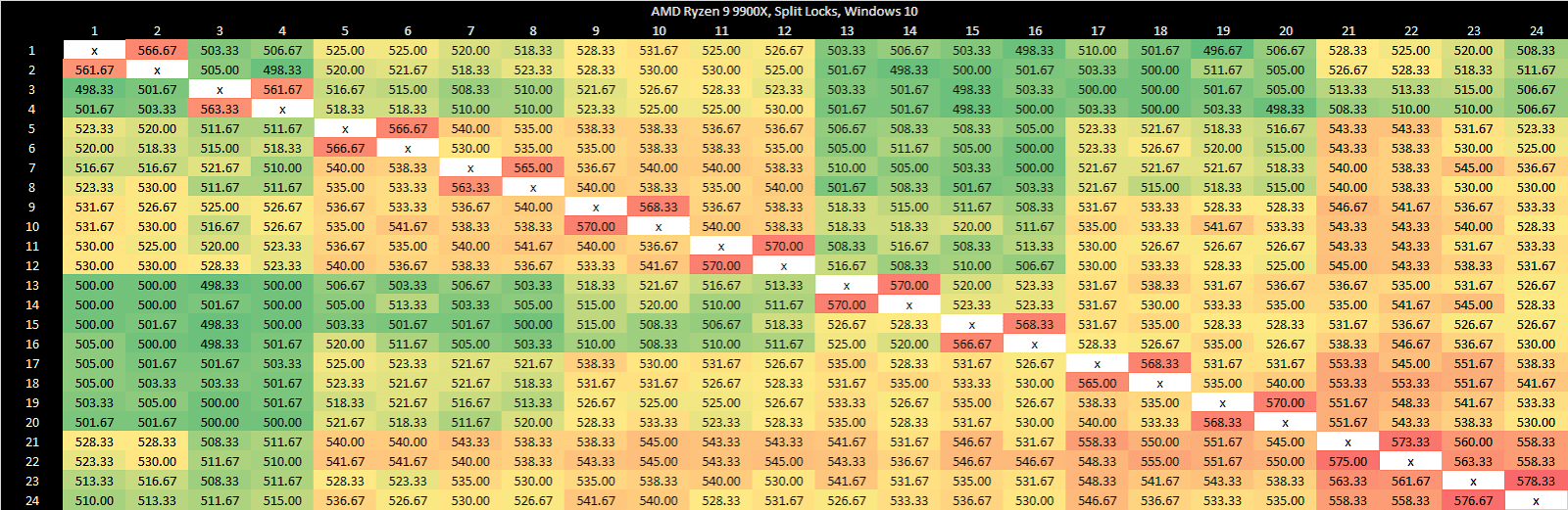
Split locks trash everything beyond L1D. L2 and L3 performance regresses by a factor of ten. Zen 5 suffers severe penalties from split locks compared to Arrow Lake, though this situation is certainly a very contrived and unrealistic one.
Both Geekbench 6 workloads take heavy performance regressions under split lock contention. Asset Compression doesn’t generate a lot of L3 miss traffic, but even a L1D miss is very costly with split locks being looped on Zen 5.
Alder Lake uses a hybrid core setup with Golden Cove P-Cores and Gracemont E-Cores. Split locks perform horribly, and also invert the latency picture compared to intra-cacheline locks. Bouncing a cache line between P-Cores normally happens with less latency than on the E-Cores. Prior to Arrow Lake, Intel had to take a trip through the ring bus even when bouncing a line between E-Cores in the same cluster.
With split locks, P-Cores suffer agonizingly poor latency. Split locks between P and E-Cores have just above 7 microseconds of latency, matching Arrow Lake. E-Cores have the best split lock latency.
Alder Lake’s memory subsystem tolerates split locks well. L3 performance only takes a modest hit. DRAM latency goes up with split locks come into play, but not by a large amount.

Geekbench 6’s photo filter and asset compression workloads barely show any performance loss, as foreshadowed by microbenchmark results. Alder Lake might have particularly poor split lock performance, but does an excellent job of insulating other applications from their effects.
Zen 2’s split lock latency lands above Zen 5’s, though it’s still better than what Intel’s newer architectures achieve. Latencies remain constant regardless of cluster boundaries, mirroring behavior seen with Zen 5 and Arrow Lake.
As on Zen 5, split locks have a devastating effect on any L1 miss. Bandwidth and latency regress by around 10x with the core to core latency test spamming split locks.
Curiously, L3 latency takes another hit after 2 MB if split locks are being looped on the same CCX. Zen 5 didn’t have an extra inflection point under split lock contention even within the same CCX.
As on Zen 5, both Geekbench 6 workloads suffer heavily under split lock contention.
Intel’s older Skylake architecture actually has better split lock latency than Arrow Lake and Alder Lake. It’s a bit worse than Zen 2, but doesn’t reach into the microsecond range.
Skylake also takes split lock contention penalties for L2 misses, but not for L2 or L1 hits.
Both tested Geekbench 6 workloads show measurable performance impact from split locks. Photo filter loses 34.24% of its performance, while asset compression takes a lower 16.2% loss.
AMD’s Piledriver has high core to core latency results, but remarkably has the best results for split locks. Split lock latency is double to triple the latency of intra-cacheline locks, but that’s worlds better than on newer platforms.
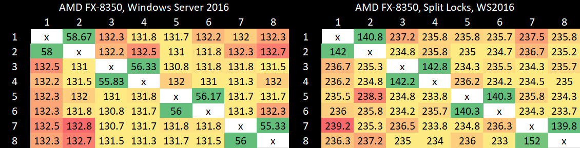
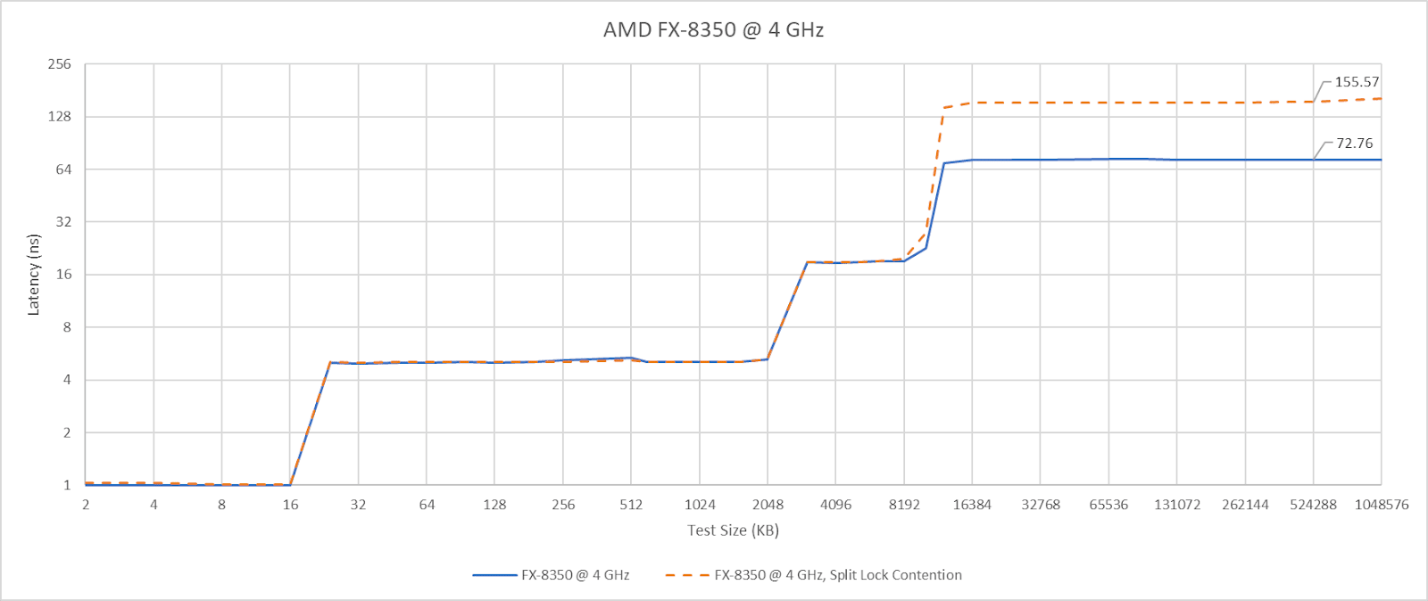
Split locks don’t affect cache hits. Remarkably, that extends to the shared L3 cache. DRAM performance does get hit, with latency doubled and bandwidth cut by more than half.
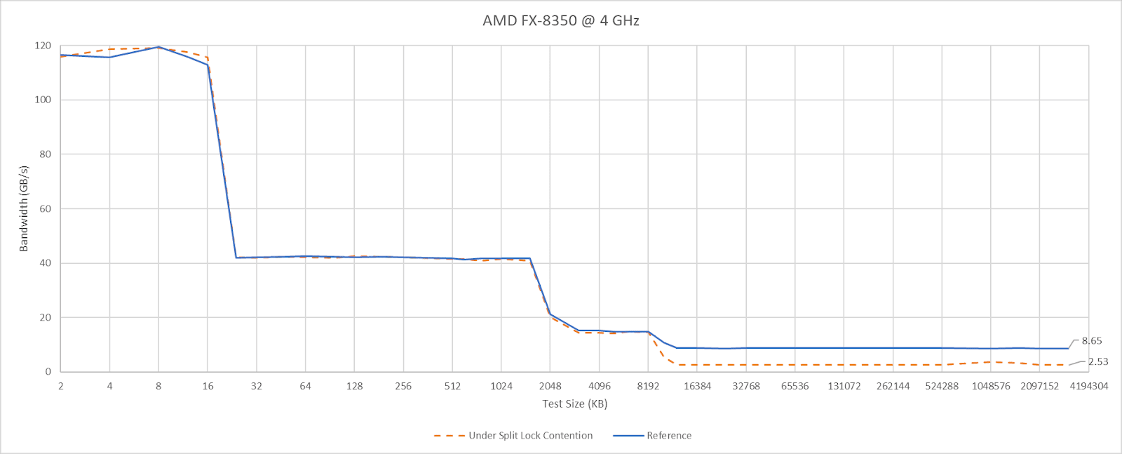
Microbenchmark results translate to higher level workloads. Geekbench 6’s photo filter and asset compression workloads both get away with only minor performance impact. The hit to DRAM performance certainly hurts, but a Piledriver core has 10 MB of cache completely unaffected by split locks. No other hardware tested here can field that much split-lock-unaffected cache capacity.
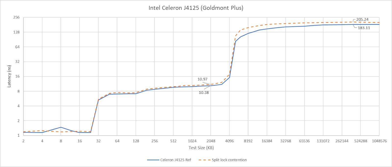
Goldmont Plus has high split lock latency, though it’s still curiously better than Intel’s more modern Arrow Lake and Alder Lake.
Just like Arrow Lake’s E-Cores, Goldmont Plus can hit L2 and be completely unaffected by split locks. DRAM bandwidth does take a substantial drop, but latency only regresses slightly. It’s worth noting that Goldmont Plus starts with very poor baseline DRAM latency though.
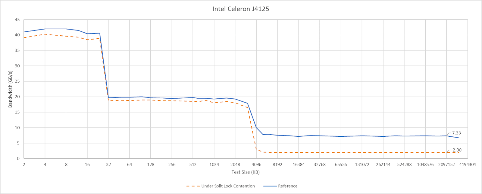
Slight differences in L1D and L2 performance can be attributed to lower clock speeds, since I didn’t underclock the chip.
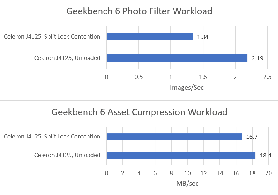
Both Geekbench 6 workloads show performance regressions, but it’s not much considering there’s also multi-core clock speed drops in the mix. Much of the score decrease for asset compression can probably be attributed to lower clocks. The photo filter workload definitely suffers, but not to the same extent as Arrow Lake or AMD’s Zen 2 or Zen 5.
The term “bus lock” dates back to early multiprocessor systems, which placed multiple CPUs on a shared bus. Each CPU had its bus pins connected to the same motherboard traces, which connected them to the chipset. Locking the bus prevents other CPUs from making memory accesses, preventing them from interfering with atomic operations. Modern CPUs no longer use a shared bus, and instead use non-blocking, distributed interconnect setups. It’s not clear what a “bus lock” really means. And while Intel and AMD still use the terminology, “bus locks” caused by split locks clearly have a range of effects depending on the hardware in question.
I suspect Intel’s bus locks are implemented in their IDI (in-die interconnect) protocol. P-Cores and E-Core use IDI to talk to the uncore, which starts with the ring bus on most Intel client designs. Goldmont Plus’s performance monitoring documentation curiously indicates that a “bus lock” is a special request to the L2 controller, though L2 hits aren’t impacted just like on other Intel designs.
AMD’s implementation goes beyond a traditional bus lock in Zen 2 and Zen 5, with core-private L2 caches impacted as well. One possibility is that AMD falls back to the Infinity Fabric layer when handling split locks, though I don’t have strong evidence to support that. Performance monitoring events increment at the Data Fabric’s Coherent Stations during core to core latency test runs. But if they’re responsible, they only handle control path traffic because the increments aren’t proportional to L2 hit traffic observed when also running a memory bandwidth microbenchmark.
Piledriver also throws a wrench into the works when trying to define bus locks. Maybe AMD’s old architecture doesn’t use bus locks at all, and is able to use its cache coherency protocol to let unrelated accesses proceed as long as they hit cache.
Overall, there’s no good analogy to the classical shared bus on a modern CPU. Perhaps CPU designers should drop the term “bus lock” from documentation, and precisely document how a split lock impacts their systems.
Linux’s split lock mitigation traps split locks and introduces millisecond level delays, aiming to both make split locks “annoying” and provide better quality of service to other applications.
Testing on Linux without touching sysctl settings shows latency comparable to mechanical hard drive seek time, which is an eternity for a CPU. This kind of delay should also eliminate the noisy neighbor effects above, since the split lock core to core latency test simply isn’t running most of the time.
I think Linux’s default makes sense for mutli-user or server systems, which value consistent performance when running a large number of tasks. Limiting noisy neighbor effects from a rogue application, like my test code above that spams split locks, is a sensible option. I can see it being used alongside other QoS mechanisms like running at lower, locked clock speeds, partitioning caches, and throttling memory bandwidth usage to ensure consistency.
For consumer systems though, Linux’s default feels like an overreaction to a problem that didn’t exist. A core-to-core latency test uses locks at a rate no normal application would. A split lock variant of that test is even more ridiculous. Games have apparently been using split locks for quite a while, and have not created issues even on AMD’s Zen 2 and Zen 5. However, a game that runs at 10 FPS on Linux and 200 FPS on Windows is a problem for Linux.
Linux traditionally struggled on the desktop scene because it required a high level of technical skill and substantial troubleshooting time from users. Linux distros have made tremendous progress in chipping away at those requirements over the past two decades. But doing a scream test on users - that is, attempting to impose a vision of the “proper” way to do things by creating an artificial performance problem - is a step backward. Ease of use is everything in the consumer world. Every OS problem that a user has to troubleshoot is a failure on the OS’s part. Going forward, I hope Linux dodges avoidable problems like this.
Split locks don’t stop other cores from running code. They’re not the hardware equivalent of Python’s global interpreter lock, or another similar construct that blocks concurrency. On modern CPUs, split locks don’t even block all memory accesses. They only introduce a performance penalty when those memory accesses miss a certain cache level. That performance penalty varies wildly too.
Applications tend to suffer varying degrees depending on how often they miss cache. Hardware has a huge influence too. AMD’s Piledriver and Intel’s Alder Lake do the best job of minimizing noisy neighbor effects. Piledriver is especially impressive because it manages that while delivering the best split lock latency across all hardware tested here. On the other hand, AMD’s Zen 2 and Zen 5 suffer heavily in this corner case. Another application could slow down so much that you’d be forgiven for thinking you got a version of it compiled using Claude’s C Compiler.
From these results, programmers should obviously strive to avoid split locks. They perform poorly, and have a heavier effect on other applications than intra-cacheline locks. From the hardware side, there’s clearly room to optimize split locks for better performance and reduced noisy neighbor effects. I hope to see both hardware and software developers take a measured, data-driven approach to tackling the split lock problem, and one that doesn’t involve introducing new performance problems.
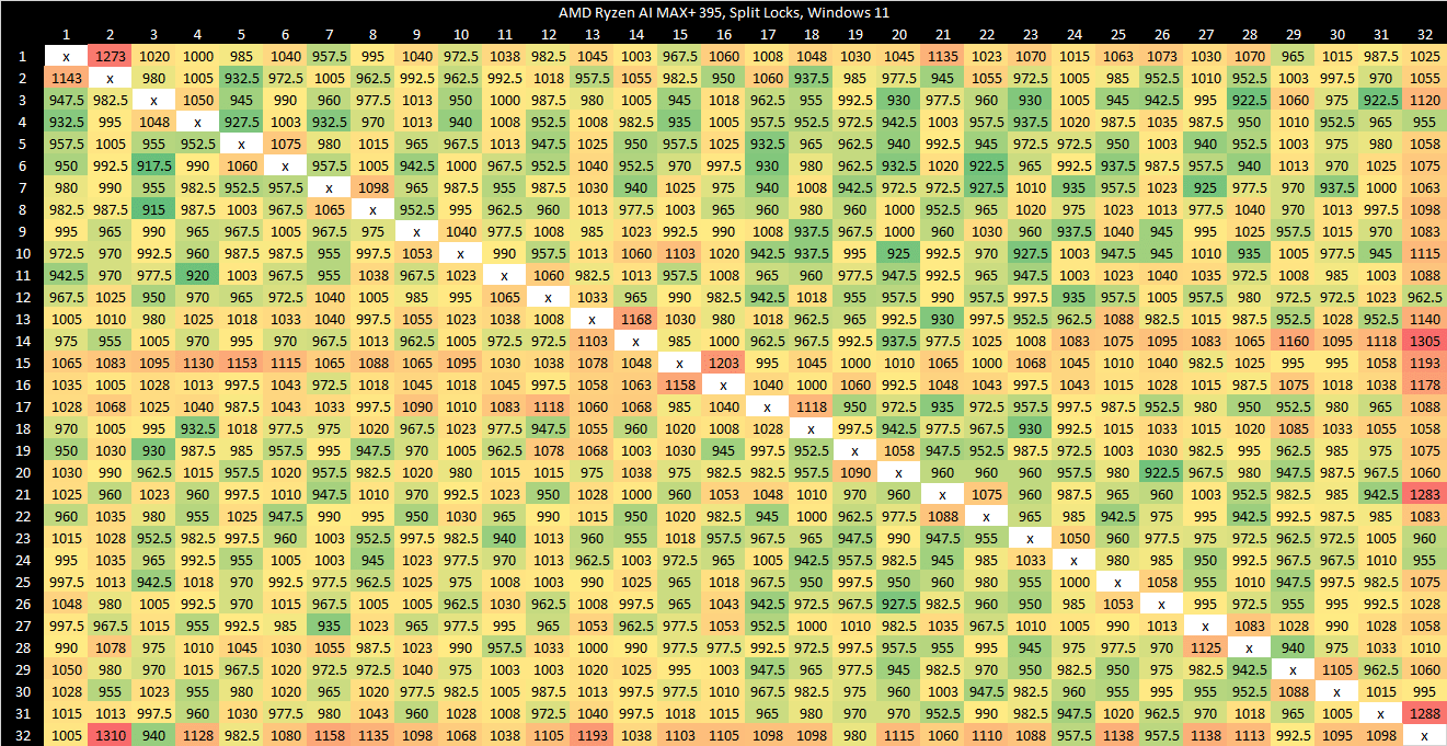
Zen 5 in the Ryzen AI MAX+ 395 (Strix Halo) has higher split lock latency than its desktop Zen 5 counterparts. I suspect split locks are handled at Infinity Fabric’s Coherent Station blocks, but curiously those counters also increment for intra-cacheline locks that are handled within a CCX. Perhaps the Coherent Station gets some sort of notification about a line changing state.
Zen 4 in a high performance mobile implementation shows similar split lock latency to Zen 2.
Arrow Lake E-Cores have a lot of monitoring sophistication around bus locks. Under the split lock core to core latency test, any E-Core involved gets blocked for nearly all cycles. However, other E-Cores are only blocked around half the time. That would explain the roughly 50% L3/DRAM performance degradation, though it does not explain how L2 performance remains unscathed.
I took rough notes on die to die traffic when running Geekbench 6 workloads on Arrow Lake by observing performance counters sampled at 1 second interval and picking out spikes. My goal isn’t to give an accurate figure for average L3 miss traffic per workload, but rather to select two interesting workloads for measuring split lock impact.
2026-04-01 15:02:33
Update (4-2-2026): After careful consideration of changing conditions, especially the change in current date, the transition to Claude’s C Compiler has been rescinded. The original article remains below.
Our society has gone all-in on AI. Software and related technologies represent one of the biggest sectors of the US economy, and technology companies have all but bet the farm on LLMs being able to do everything under the sun. By the law of sunk costs*, AI investments will increase without bound until that objective is achieved. AGI is therefore inevitable, and everyone must fully commit to ensuring AI’s success because things will get more painful the longer it takes. When bank money runs out, the government will bail them out. When government funds are exhausted, aliens will get involved, followed by various deities. Please don’t ask what happens after that. Anyway, it’s in everyone’s best interest to embrace the AI revolution with absolute conviction. Therefore, I’m excited to announce that Chips and Cheese will stand at the vanguard of the AI revolution by adopting Claude’s AI-generated compiler, CCC.
CCC, or Claudes’ C Compiler, is a “from-scratch optimizing compiler with no dependencies […] able to compile the Linux kernel.” Anthropic used their Claude large language model (LLM) to write the entire compiler. Human effort was relegated to prompting and maintaining AI coding agents, and standing up a very robust test suite to keep those coding agents on track. Past Chips and Cheese articles used microbenchmarks and benchmarks built using GCC. GCC was developed by humans, which is backwards and reactionary by the standards of many cadres today. Comparing GCC and CCC should be a powerful showcase of revolutionary software development practices.
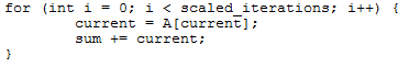
Microbenchmarking is a useful tool for understanding low level hardware characteristics like cache and memory latency. My first shot at testing load latency used a simple loop of dependent array accesses in C:
A = A[current] creates a dependency chain where one array access result feeds into the next, preventing accesses from overlapping even on an out-of-order core. Dividing access time by iteration count gives latency. CCC and GCC compile the loop into the following assembly code:
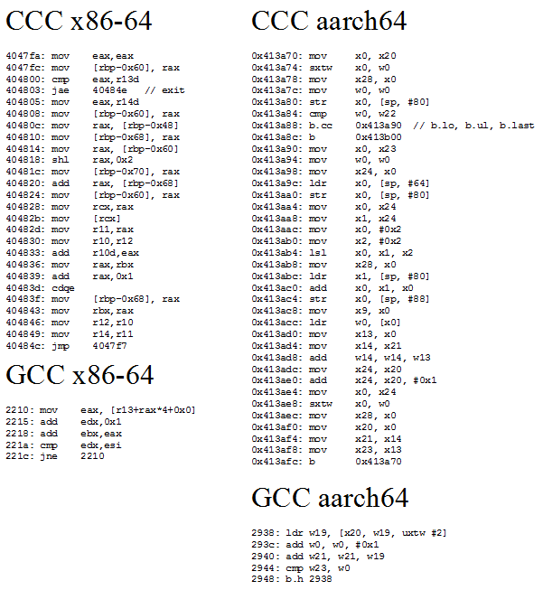
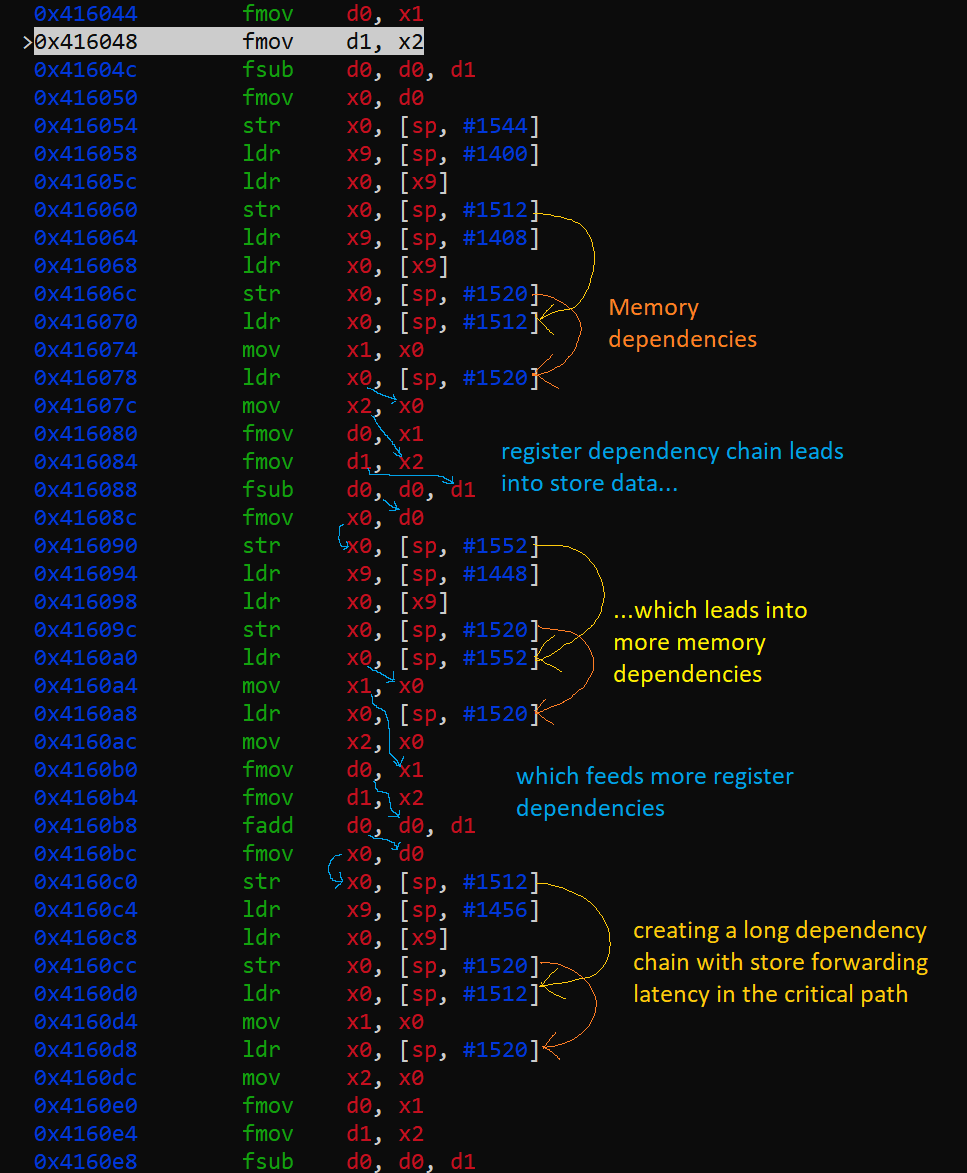
CCC generates more code from the same high level source than GCC does, and sometimes, more is better. CCC’s code is more ideologically correct from a RISC standpoint. GCC uses indexed addressing modes that express a dependent shift, add, and load sequence in a single instruction. RISC advocates for a small set of simple instructions and larger code sizes, and indexed addressing modes are quite complex. CCC follows the RISC philosophy, and splits the array access into separate shift, add, and load instructions.
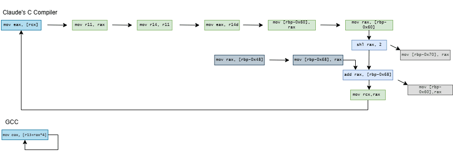
CCC doesn’t stop there and exceeds quotas by decomposing current = A[current] into a nine instruction dependency chain. On x86-64, it shuffles the index through several registers and sends it on a trip through the stack. It does the same on aarch64, but at least keeps the index in registers. On both architectures, CCC brings the array base address in from the stack, and sends it on another round trip through the stack for good measure before using it.
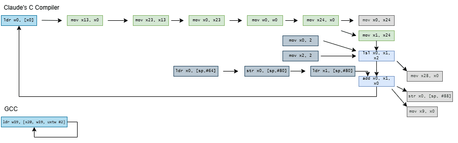
Compiling the microbenchmark with CCC results in higher observed array access latency. Zen 5 and Lion Cove need two extra cycles, likely from the shift + add dependency chain. Exceptionally strong move elimination and zero-latency store forwarding seem to let Intel and AMD collapse the nine-instruction dependency chain. After that, their out-of-order core width absorbs the additional instructions. Arm’s recent cores have less robust move elimination and can’t do zero latency store forwarding. They suffer a 6-7 cycle penalty.
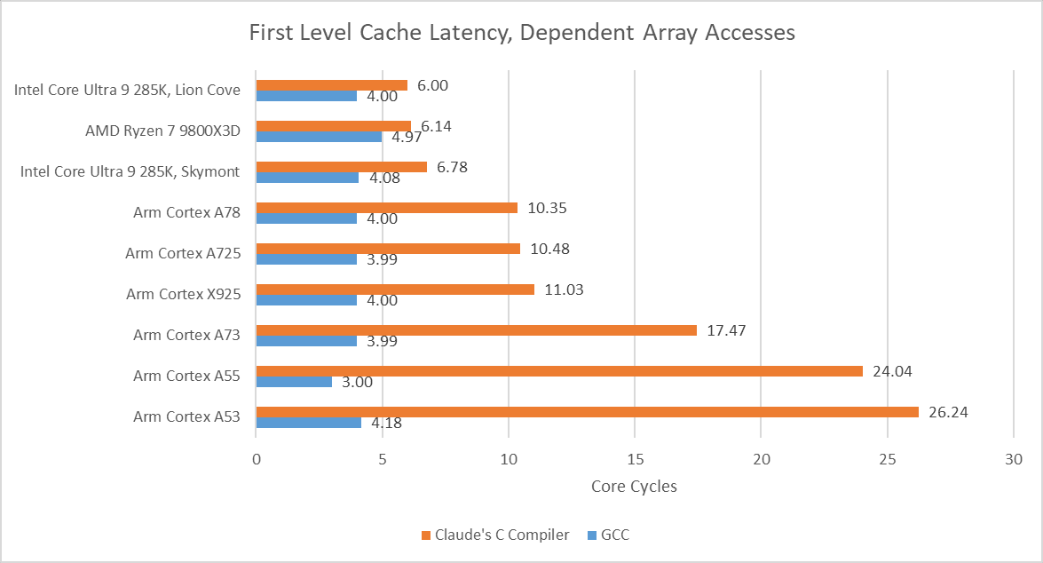
Smaller cores with narrower execution engines struggle with CCC-compiled code, likely because they don’t have enough core throughput to absorb loop overhead and the sum += current sink statement. CCC also compiles those into very long assembly sequences, placing pressure on core throughput.
In-order cores suffer the largest penalties. They’re not embracing the AI revolution with adequate enthusiasm, and should seriously reconsider their stance or risk getting denounced.
Old, traditional compilers force the masses to follow a tight set of rules dreamt up by the bourgeoisie. If a programmer doesn’t follow these rules, the compiler will complain and may even refuse to complete the compilation process. Warnings and errors are of no use to the proletariat, who just want results. CCC boldly crushes type systems with revolutionary fervor, as if to shout “out with the old, in with the new!” Take the following code:
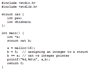
GCC cowers behind error messages with weak excuses about incompatible types and fails to produce a binary. In doing so, GCC engages in counter-revolutionary wrecking by undermining the work of the masses, who have to waste time fixing errors.
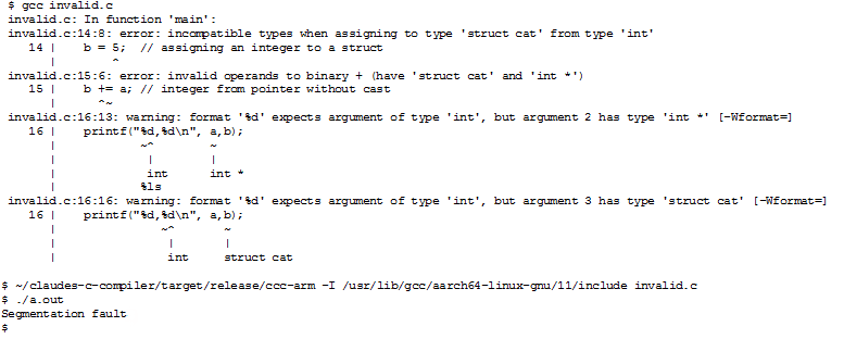
Rather than make excuses, CCC raises the revolutionary banner high and produces an executable.
Claude’s C Compiler only compiles C code. All other languages are therefore invalid. Eight of SPEC CPU2017’s workloads are C-only. I tested them on the following cores:
Arm Cortex X925 in Nvidia’s GB10
AMD Zen 5 in the Ryzen 7 9800X3D, with boost disabled
Intel Lion Cove in the Core Ultra 9 285K
I ran with boost disabled on the 9800X3D because running CCC-built workloads takes a lot of time. Extra time spent in high performance states mean more power consumption, and we should save every last bit of power possible to feed AI applications.
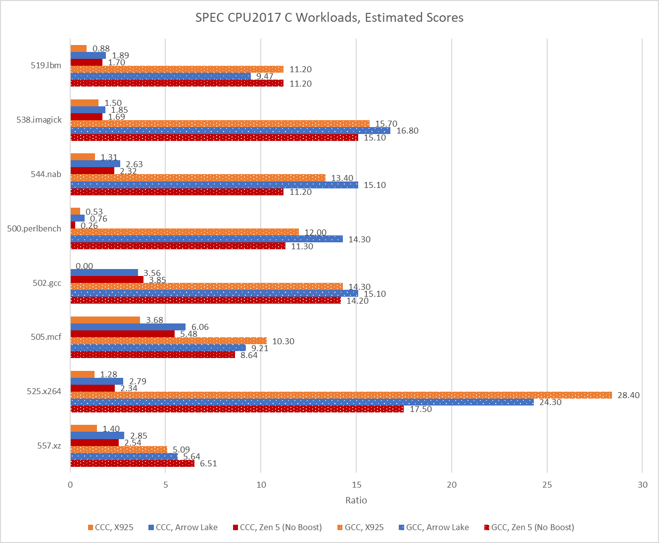
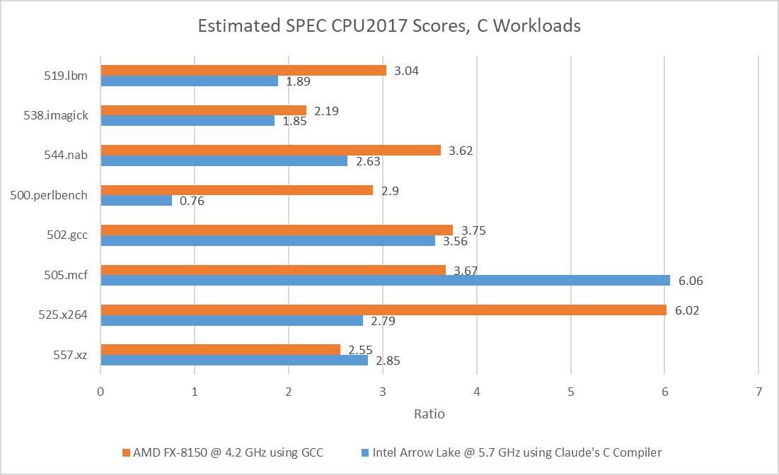
CCC’s version of 502.gcc consistently crashed with a segmentation fault on Cortex X925, even though it managed to complete some runs on x86-64. When it ran to completion on x86-64, CCC’s 502.gcc delivered 23.6% and 27.1% of the performance of its GCC-compiled counterpart on Lion Cove and Zen 5, respectively. CCC hit its relative performance peak on 505.mcf, where it managed less than a 35% regression versus GCC. Across the eight tested SPEC CPU2017 workloads, using CCC on average regressed performance by somewhere above 70%.
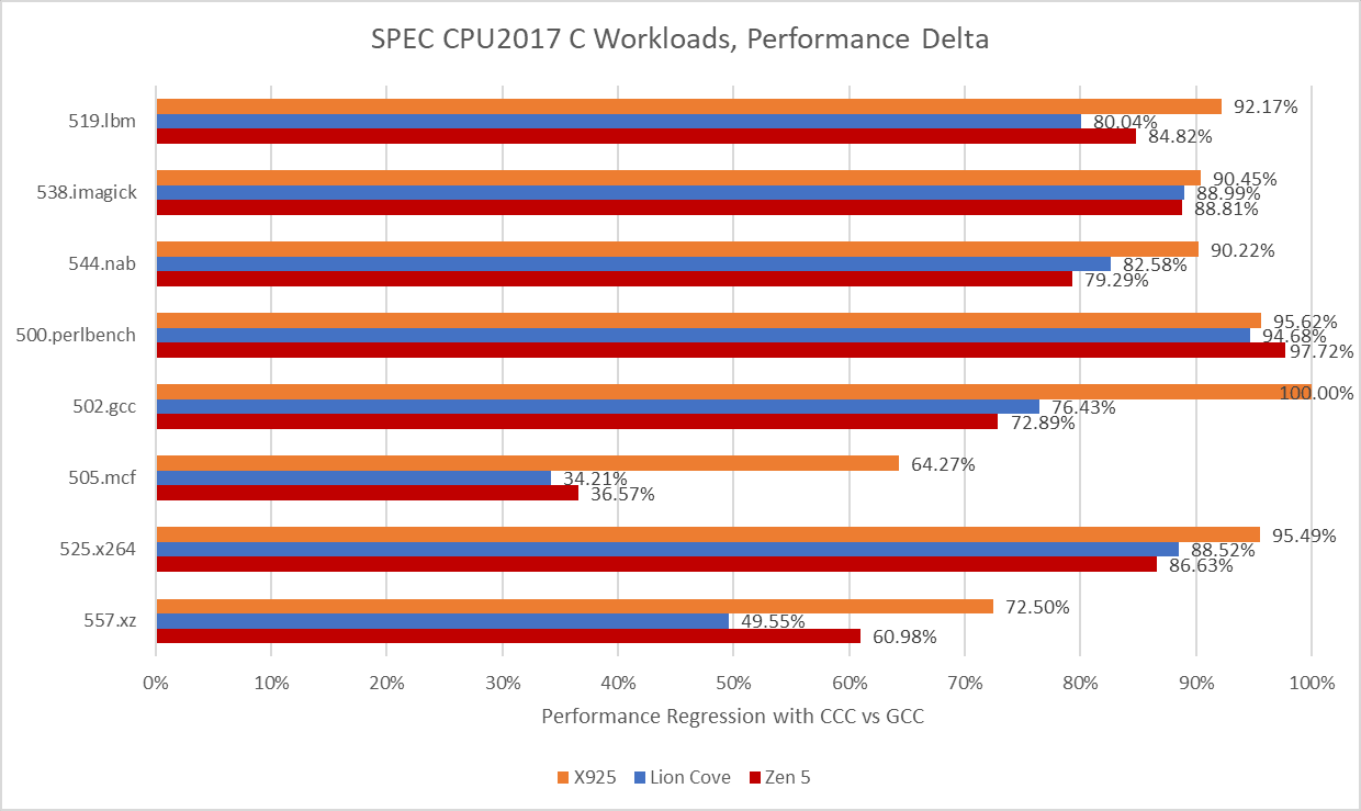
Arm’s Cortex X925 suffers hardest from the CCC switch. With GCC, Arm’s core was very much a match for Zen 5 and Lion Cove. Now, it loses in every workload except for 500.perlbench, where Zen 5 takes a dive to let X925 slip ahead. But X925 still can’t compare to Lion Cove in that workload.
In turn, Lion Cove can’t compare to Sun’s UltraSPARC IV+. SPEC CPU2017 scores are speedup ratios relative to a reference machine, which is “a historical Sun Microsystems server, the Sun Fire V490 with 2100 MHz UltraSPARC-IV+”. Lion Cove may have the best 500.perlbench score of the three cores tested here at 0.76, but that’s below 1. A vibe-coded compiler is the product of the latest software development techniques and can’t be at fault. It therefore follows that Sun’s UltraSPARC-IV+ is amazing. The UltraSPARC-IV+ is a dual core version of the UltraSPARC III, which uses a 4-wide in-order pipeline. Lion Cove is an 8-wide out-of-order design with massive reordering capacity and much higher clock speeds, but clearly none of that is necessary to win.
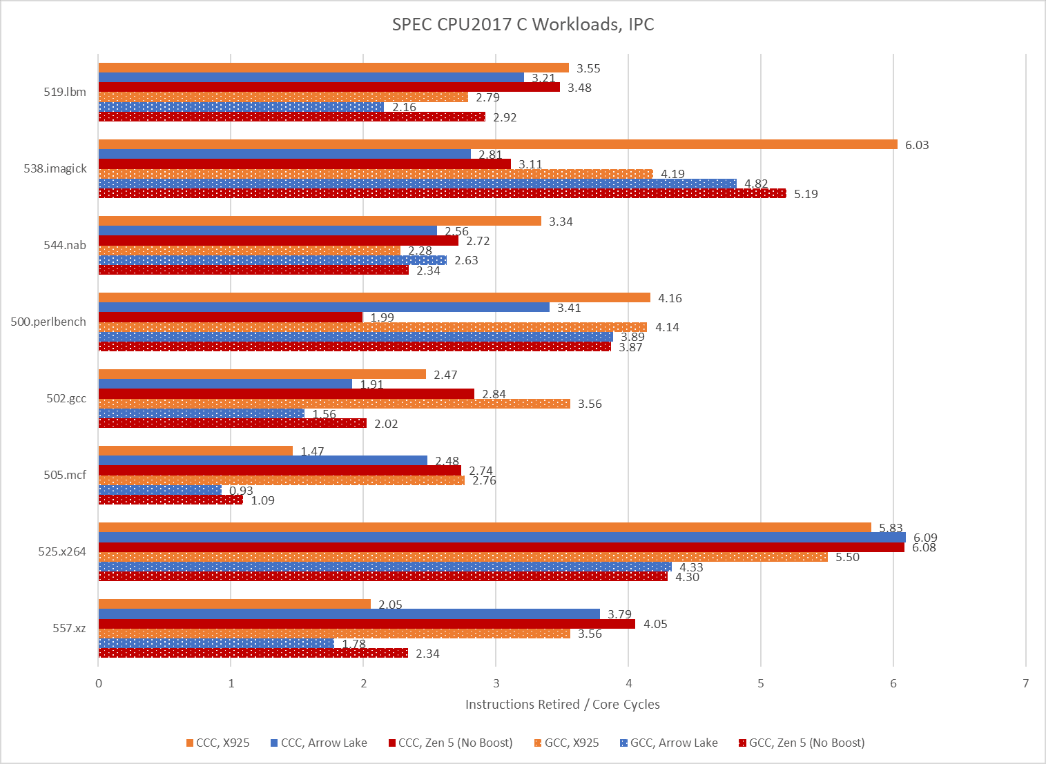
Performance is overrated. Analysts today agree that IPC is more important than performance, and CCC code achieves excellent IPC. On 525.x264, Arrow Lake averages 6.09 IPC when running CCC code. That’s the highest IPC average across all SPEC CPU2017 runs above. GCC’s best IPC average tops out at a wimpy 5.5. CCC’s IPC advantage isn’t universal though, and GCC does manage higher IPC on 538.imagick.
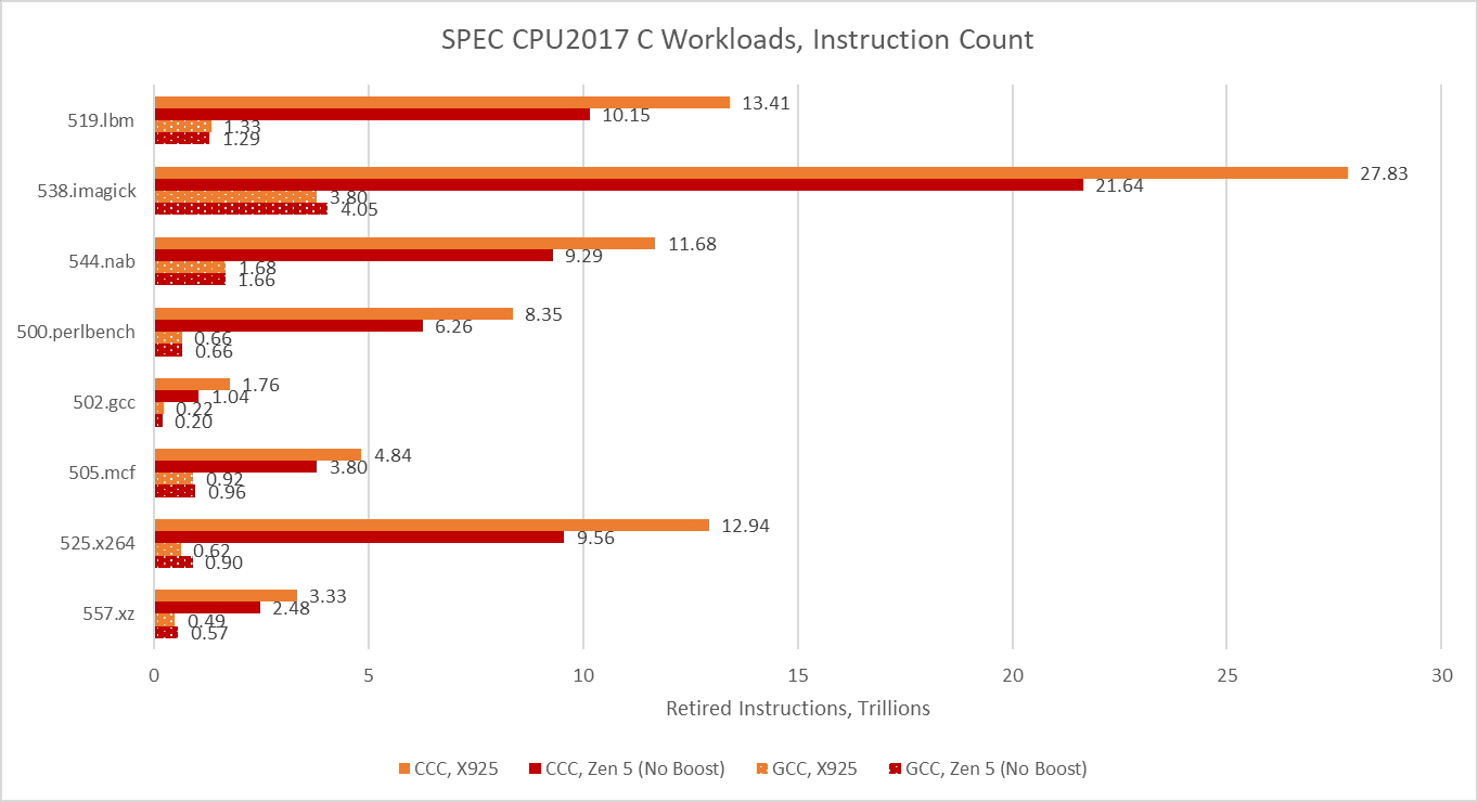
As foreshadowed with the cache and memory latency microbenchmark, CCC takes a great leap forward in instruction counts across all eight SPEC CPU2017 workloads. Some workloads execute more than 10x as many instructions.
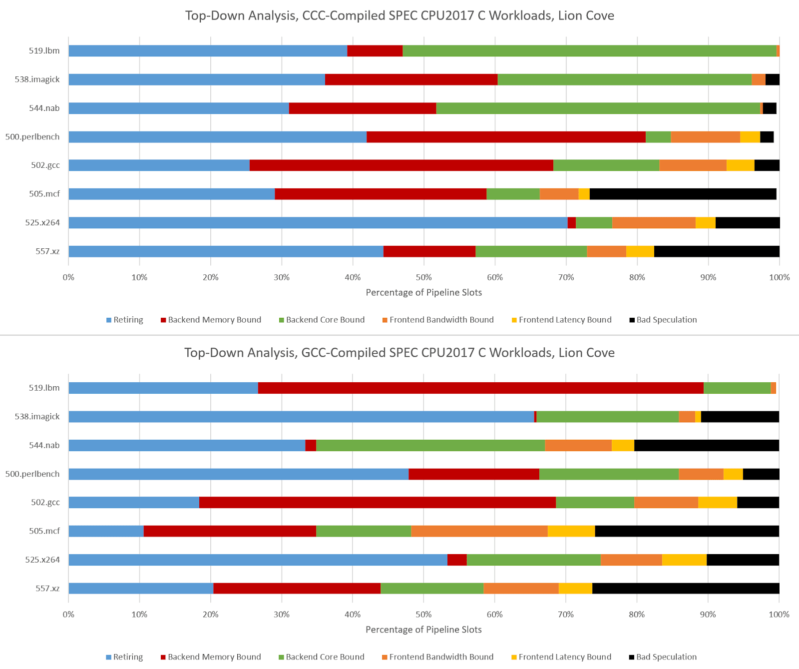
Hardware performance monitoring reveals a different set of challenges for the CPU pipeline when comparing GCC- and CCC-compiled code. Branch prediction is less important because branch count didn’t grow proportionately to total instruction count. SPEC CPU2017’s three C-only floating point workloads become very core-bound when built with CCC. On Zen 5, that means retirement is blocked by an instruction that doesn’t read from memory. That indicates performance is limited by how fast the core can execute instructions, rather than how fast the memory subsystem can feed the core with data. The five integer workloads become less frontend bound, and face steeper backend challenges. CCC workloads across the board achieve higher core utilization than their GCC-compiled counterparts, as the IPC figures from before suggest.
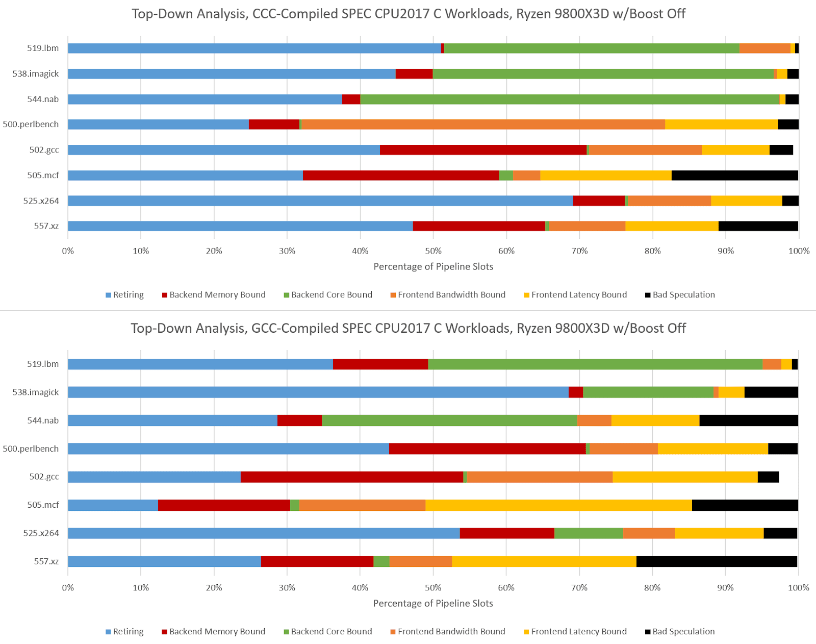
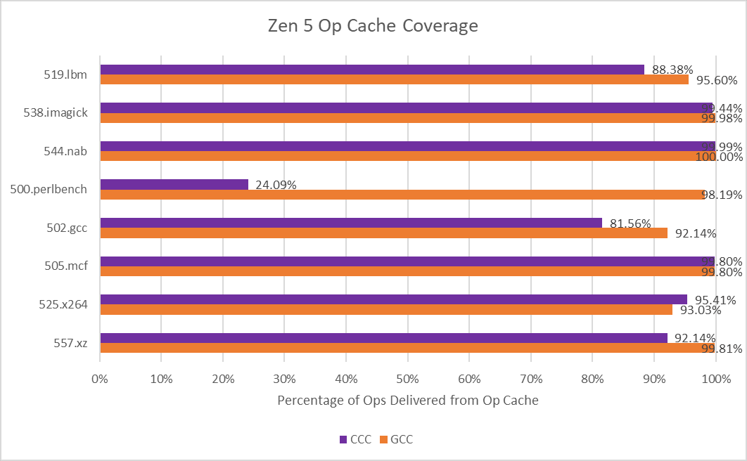
500.perlbench is a catastrophically bad case for Zen 5 when compiled with CCC because of a much lower op cache hitrate. Zen 5 primarily feeds itself with a 6K entry, 16-way op cache, which can fully feed the 8-wide rename/allocate stage. 4-wide, per-thread decoders handle larger instruction footprints. Typically applications with poor code locality suffer from other IPC limiters besides frontend throughput, especially when the core isn’t running a second thread that can hide latency. 500.perlbench has higher IPC potential if not for the per-thread decode throughput limitation, putting Zen 5 behind X925 and very far behind Lion Cove. It’s the first case I’ve seen outside a microbenchmark where Zen 5’s decoder arrangement comes out to bite. Zen 5’s op cache manages high coverage in other workloads, so 500.perlbench is an exceptional case.
CCC challenges Lion Cove’s pipeline in a similar fashion, though Lion Cove is generally more backend bound than Zen 5. This could be because Lion Cove sits atop a higher latency uncore. Or, the difference could be down to accounting methodology. For example, Intel might be counting cycles where any instruction is delayed by a load as “memory bound”, which could lead to higher counts than AMD’s approach. Lion Cove’s 8-wide decoder excels in 500.perlbench, where frontend limitations are minor compared to what they were in Zen 5.
Arm’s Cortex X925 is very core-bound when running CCC code, and not just in the three FP workloads. I’m distinguishing between core and memory bound backend bound slots by looking at the proportion of backend bound cycles covered by the STALL_BACKEND_MEMBOUND event, which counts when there’s a backend stall and the “backend interface to memory is busy or stalled”.
I partially attribute the core-bound slot increase to Cortex X925 not having the robust move elimination and zero-latency store forwarding that Lion Cove and Zen 5 do. Long chains of register-to-register MOVs or frequent trips through the stack are rare in typical code. As evidence, Intel's Ice Lake only took a 1-3% performance loss with move elimination disabled. Move elimination therefore acts as a cherry on top in most applications, with most performance coming from out-of-order execution basics and an efficient cache hierarchy to feed the core. Of course, that changes with CCC.
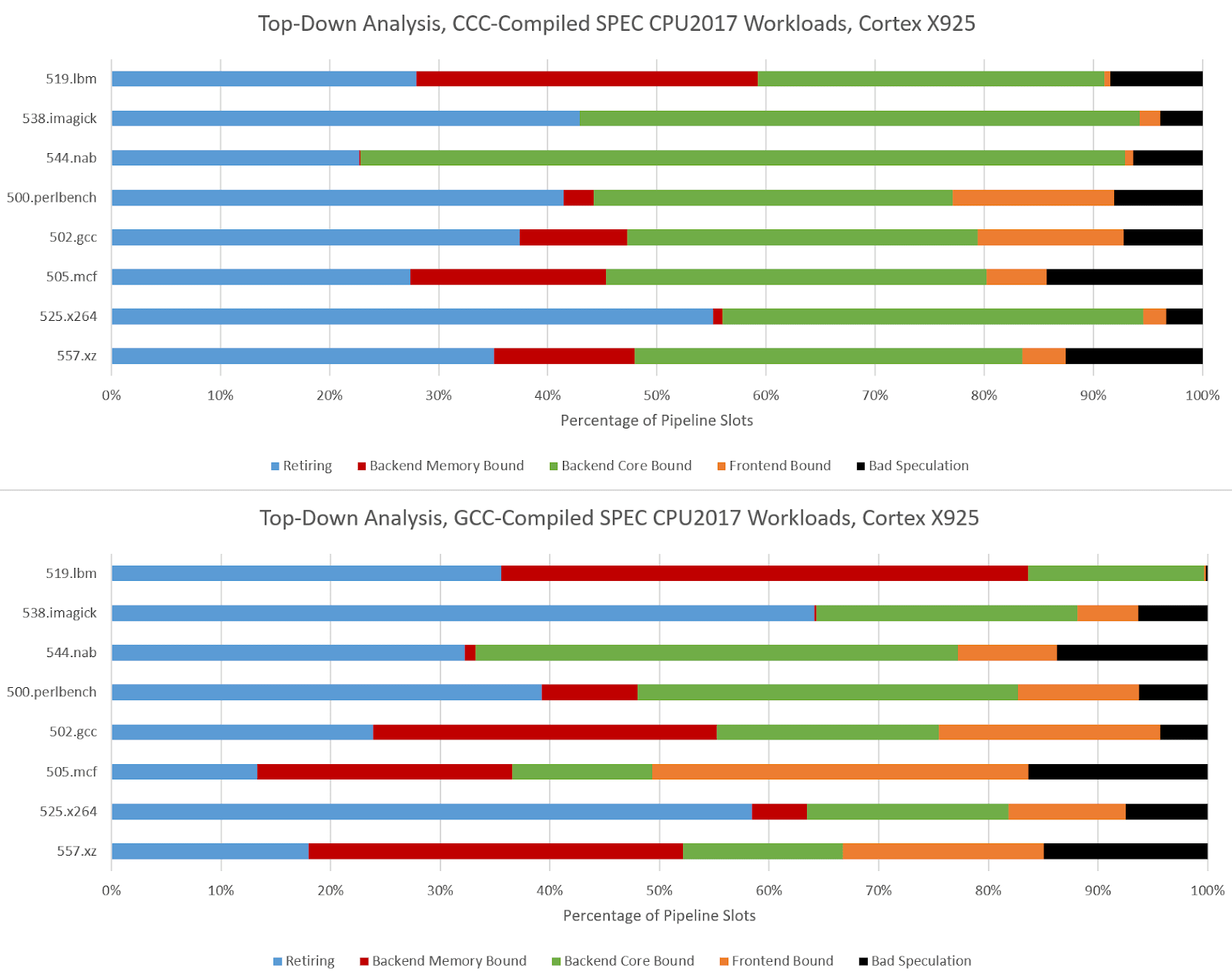
519.lbm’s large increase in backend memory bound slots looks related to store forwarding latency. A hot section in CCC-compiled 519.lbm repeatedly spills register x0 to the stack, only to reload it several instructions later, making sure the memory system contributes to all phases of code execution. Store forwarding latency forms part of a long dependency chain, and X925 can’t do zero-latency forwarding the way Zen 5 and Lion Cove can.
Compilers are crucial to modern software development, and performance of compiled code is key to making high level languages practical. Switching to CCC causes a 70%+ performance degradation across C-only SPEC CPU2017 workloads. Most consumers will readily accept this, because a fast core like Intel’s Lion Cove still does well when running CCC code. As evidence, AMD’s Bulldozer architecture fascinated enthusiasts about 15 years ago. Bulldozer is 36.8% faster than Lion Cove, the fastest CPU tested here for running CCC code. Simply overclocking Lion Cove to 8 GHz could close much of the performance gap.
Of course, some provocateurs may only reach 7.5 GHz, undoubtedly due to a combination of personal skill issues and insufficient enthusiasm for the AI revolution. Severe agitators may theorize that Bulldozer’s level of single threaded performance is not top-notch in some scenarios, and demand ever more performance. To prevent these people from discrediting the revolution, the stock performance problem must be addressed.
Performance problems can be addressed from either hardware or software, because hardware and software optimization go hand-in-hand. Well optimized software performs well across a wide variety of hardware. Likewise, well designed hardware delivers good performance across a wide range of software. CCC-generated code dramatically shifts what software demands from hardware, upsetting the existing social contract between software and hardware. Faulting the software side would undermine the crowning achievements of the AI revolution. Therefore, hardware must boldly tackle the performance question.
Completely addressing the performance gap would be easy by my estimate. With 20-30 GHz clock speeds and several generations worth of architectural improvements, CCC code could reach the performance achieved by GCC-compiled binaries on current generation hardware. These targets might have been dismissed in the past. But they’re achievable now because the AI revolution isn’t just any revolution. Rather, it is a cultural revolution that upends views regarding power consumption. Infinite power can make many previously unthinkable designs a reality. Some hardware designers may see red flags in this approach and persistently complain. But proper hardware engineers will rally around those flags and chant slogans. By correctly following the path of the revolution, they’ll be sure to succeed and may even exceed their quotas. May the odds be ever in their favor.
* The proof is trivial and similar to the proof for the gambler’s law (99% of gamblers quit just before they win big)